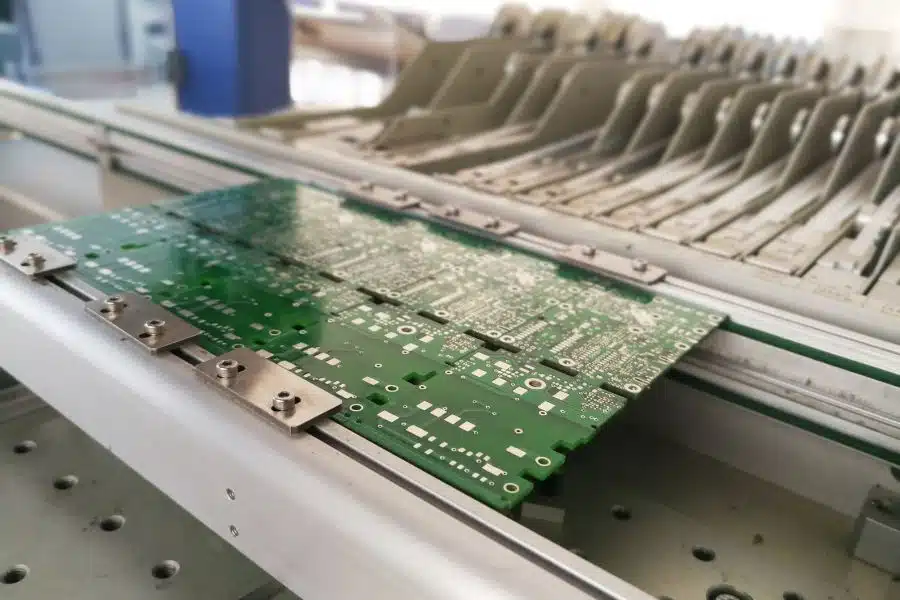
A professional PCB assembly process transforms a bare printed circuit board into a reliable, fully functional electronic assembly. From SMT stencil fabrication, solder paste printing, and component placement to reflow soldering, AOI inspection, X-ray inspection, and functional testing, every stage directly affects the quality, reliability, and performance of the finished PCBA.
Whether you need a few engineering prototypes, a small-batch build, or high-volume production, understanding the complete PCB assembly process helps engineers, procurement teams, and product manufacturers select the right manufacturing strategy and reduce production risks.
As an experienced PCB manufacturer and PCB assembly service provider, Kingda provides professional PCB prototype manufacturing, quick-turn PCB prototyping, and PCB assembly solutions, supporting customers from initial design verification through production. Our manufacturing approach combines engineering review, controlled assembly processes, inspection, testing, and continuous process improvement to help customers achieve stable and consistent PCBA quality.
Table of Contents
- Creating the SMT Stencil
- Applying Solder Paste
- Component Placement
- Reflow Soldering
- Automated Optical Inspection (AOI)
- Statistical Process Control (SPC)
- X-Ray Inspection (AXI)
- Selective Soldering for THT Components
- Final Inspection, Cleaning, and Packaging
- Functional Testing and Continuous Improvement
- Key Equipment and Manufacturing Capabilities
- Why Choose Kingda for PCB Assembly?
What Is the PCB Assembly Process?
The PCB assembly process, commonly referred to as PCBA, is the manufacturing process of mounting electronic components onto a bare PCB and soldering them to create a functional electronic circuit.
A typical assembly workflow includes:
PCB Design → DFM Engineering Review → SMT Stencil → Solder Paste Printing → Component Placement → Reflow Soldering → AOI Inspection → X-Ray Inspection → THT/Selective Soldering → Cleaning → Functional Testing → Final Inspection → Packaging
Depending on the product design, component types, production volume, and reliability requirements, some steps may be combined, repeated, or performed in a different sequence.
For engineers, particular attention should be paid to PCB design for manufacturing (DFM), stencil design, solder paste deposition, component placement, reflow profiling, AOI, and X-ray inspection.
For procurement teams and product managers, production scalability, component sourcing, quality control, traceability, testing capabilities, lead time, and packaging are equally important.
At Kingda, the assembly process is designed to support different production requirements, including PCB prototyping, low-volume PCB assembly, medium-volume production, and high-volume PCB assembly.
Step 1: Creating the SMT Stencil
Before solder paste can be applied, an SMT stencil must be prepared according to the PCB pad layout.
The stencil is normally manufactured from stainless steel and contains precisely designed apertures corresponding to the solder pads on the PCB. During solder paste printing, these openings determine where and how much solder paste is deposited.
What Happens?
The manufacturing team reviews the PCB layout, component package information, pad geometry, and production requirements before preparing the stencil.
For fine-pitch components, BGA packages, QFNs, and miniature passive components, stencil aperture design becomes particularly important.
Factors that may be considered include:
- Pad dimensions
- Component pitch
- Stencil thickness
- Aperture size and shape
- Area ratio
- Paste volume
- Component spacing
- PCB surface finish
- Lead-free solder requirements
Why Does the SMT Stencil Matter?
The stencil directly controls the amount and position of solder paste deposited on each pad.
If an aperture is too large, excessive solder paste may cause solder bridging. If it is too small, insufficient paste can result in weak solder joints or open circuits.
For fine-pitch applications, optimized aperture design can significantly reduce common defects such as:
- Solder bridging
- Insufficient solder
- Solder balls
- Open solder joints
- Component tombstoning
- Uneven solder deposition
Kingda Advantage
Kingda combines PCB manufacturing and PCB assembly experience to improve manufacturability before production begins. During the engineering review, the PCB layout, pad design, component spacing, and assembly requirements can be evaluated together to reduce manufacturing risks.
This integrated approach is particularly useful for prototype PCB assembly and new product introduction, where design problems discovered before production are significantly easier and less expensive to correct.
Step 2: Applying Solder Paste
Once the stencil is prepared, the PCB enters the solder paste printing stage.
A solder paste printer positions the stencil accurately over the PCB. A squeegee then moves across the stencil, forcing solder paste through the apertures and onto the corresponding PCB pads.
For lead-free electronics manufacturing, SAC305 solder paste is widely used, although the specific alloy and paste formulation should be selected according to the product and process requirements.
Solder Paste Inspection
After printing, Solder Paste Inspection (SPI) can be used to verify the quality of the deposited solder paste.
Typical SPI parameters include:
- Paste volume
- Paste height
- Paste area
- Pad coverage
- Printing offset
- Deposit shape
- Excess or insufficient solder paste
Why Does Solder Paste Printing Matter?
Solder paste printing is one of the most important stages in SMT assembly because solder paste quality directly affects subsequent component placement and solder joint formation.
Too little solder paste may produce weak or incomplete joints, while excessive paste can create shorts between adjacent pads.
A controlled printing process helps improve:
- First-pass yield
- Solder joint consistency
- Component placement stability
- Reflow soldering quality
- Long-term product reliability
Kingda Advantage
At Kingda, solder paste printing can be integrated with inspection and process control to identify printing deviations before components are placed.
For prototypes and small-batch production, engineering feedback can also be used to optimize stencil parameters before scaling up to larger production volumes.
Step 3: Component Placement
After solder paste printing, the PCB moves to the component placement stage.
High-speed pick-and-place machines automatically collect electronic components from reels, trays, or feeders and position them onto the solder-pasted PCB pads.
The placement program is generated from PCB design data and component information.
What Happens?
The placement system uses optical vision technology to:
- Identify PCB fiducial marks
- Verify component orientation
- Correct component position
- Rotate components accurately
- Place components onto designated pads
- Detect certain component or feeder abnormalities
Modern SMT equipment can handle a wide range of components, from small passive devices to complex IC packages.
Depending on the production requirements, assembly may include:
- 0201 components
- 0402 components
- QFPs
- QFNs
- BGAs
- CSPs
- Connectors
- Power components
- Large IC packages
Why Does Component Placement Matter?
Placement accuracy directly influences solder joint quality after reflow.
Misalignment may result in:
- Tombstoning
- Open solder joints
- Solder bridging
- Incorrect polarity
- Poor electrical contact
- Mechanical interference
For high-density PCB designs, placement accuracy becomes especially important because component spacing and solder pad dimensions may be extremely small.
Kingda Advantage
Kingda supports automated SMT component placement for different production volumes and PCB designs.
For new products, engineering review can verify component libraries, placement data, polarity information, package specifications, and manufacturing requirements before mass production.
This helps reduce placement-related defects and supports a smoother transition from PCB prototype assembly to volume manufacturing.
Step 4: Reflow Soldering
After component placement, the PCB enters the reflow soldering process.
During reflow, the PCB passes through a controlled heating system. The solder paste gradually changes from a solid paste into a molten solder alloy and then solidifies, creating mechanical and electrical connections between the components and PCB pads.
A typical lead-free reflow process includes several thermal stages.
| Reflow Stage | Typical Temperature Range | Main Purpose |
|---|---|---|
| Preheat | 150–180°C | Gradually increases PCB temperature and activates flux |
| Soak | 180–200°C | Promotes thermal uniformity across the PCB |
| Reflow | Approximately 235–245°C peak | Melts solder alloy and forms solder joints |
| Cooling | Controlled ramp-down | Solidifies solder and minimizes thermal stress |
The exact profile should always be determined according to the solder paste manufacturer’s recommendations and the PCB/component construction.
Reflow Profile Optimization
The thermal profile depends on several factors:
- PCB thickness
- Number of copper layers
- Copper distribution
- Component density
- Component thermal sensitivity
- PCB surface finish
- Solder paste type
- Lead-free requirements
An improperly controlled reflow profile may cause:
- Cold solder joints
- Component damage
- Solder balls
- Bridging
- Voiding
- Pad lifting
- Warpage
- Thermal stress
Kingda Advantage
Kingda can perform engineering-based reflow profile optimization for new PCB assemblies.
Before production, the thermal profile can be evaluated against the selected solder paste and PCB construction to help establish stable process parameters.
For demanding applications, reflow process documentation can also support production traceability and quality verification.
Step 5: Automated Optical Inspection (AOI)
After reflow soldering, the assembled PCB undergoes Automated Optical Inspection (AOI).
AOI systems use high-resolution cameras and image-processing algorithms to inspect components and visible solder joints.
What Can AOI Detect?
AOI can identify many common assembly defects, including:
Component Defects
- Missing components
- Incorrect components
- Misaligned components
- Rotated components
- Incorrect polarity
- Component placement deviations
Solder Defects
- Solder bridging
- Insufficient solder
- Excessive solder
- Solder balls
- Tombstoning
- Open solder joints
- Abnormal solder fillets
For high-density boards, 3D AOI can provide additional information about solder height, shape, and volume.
Why Is AOI Important?
AOI provides an early quality gate after SMT reflow.
Detecting defects immediately allows manufacturers to:
- Prevent defective boards from moving downstream
- Reduce rework costs
- Identify recurring process problems
- Improve first-pass yield
- Support production traceability
- Provide inspection records
However, AOI cannot fully inspect hidden solder connections underneath packages such as BGAs and some QFNs. These applications may require X-ray inspection.
Kingda Advantage
At Kingda, AOI inspection can be incorporated into the SMT production workflow to identify visible assembly defects quickly and consistently.
Combined with SPI, reflow control, and engineering analysis, AOI data can help create a closed-loop quality control system for PCB assembly manufacturing.
Step 6: Statistical Process Control (SPC)
Statistical Process Control (SPC) is a data-based quality management method used to monitor manufacturing processes and identify process drift before it develops into significant defects.
Unlike a single inspection operation, SPC can collect and analyze process data throughout PCB assembly.
Typical data sources include:
| Data Source | Parameters Monitored |
|---|---|
| SPI | Paste volume, height, area, alignment |
| Pick-and-Place | Placement accuracy and machine performance |
| Reflow | Peak temperature, soak time, ramp rate |
| AOI | Defect type, location, frequency |
| Testing | Electrical and functional test results |
Process engineers can use control limits and statistical analysis to identify abnormal trends.
For example, if solder paste alignment gradually moves away from the target position, SPC can detect the trend before it creates widespread soldering defects.
Benefits of SPC
A well-managed SPC system helps improve:
- First-pass yield
- Process consistency
- Production stability
- Defect prevention
- Traceability
- Corrective action
- Continuous improvement
Instead of simply discovering defects after production, SPC focuses on identifying the conditions that may cause defects.
Kingda Advantage
Kingda emphasizes process control throughout the PCB assembly workflow rather than relying only on final inspection.
By analyzing SPI, placement, reflow, AOI, and testing information, engineers can identify process abnormalities and implement corrective actions earlier.
This approach is particularly valuable for automotive PCB assembly, medical PCB assembly, industrial electronics, and other applications where stable production is essential.
Step 7: X-Ray Inspection (AXI)
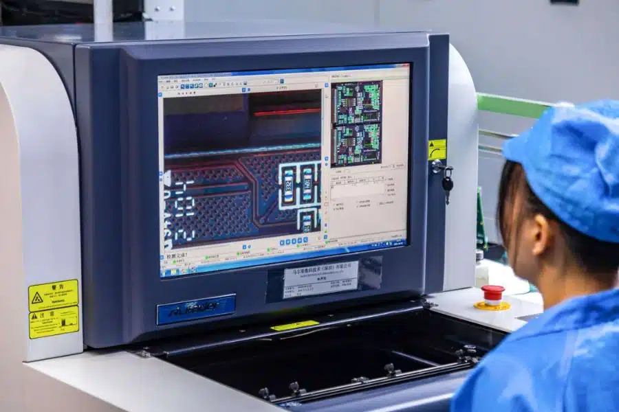
While AOI primarily examines visible components and solder joints, Automated X-Ray Inspection (AXI) can inspect hidden connections that optical systems cannot see.
X-ray inspection is especially important for assemblies containing:
- BGAs
- QFNs
- LGAs
- CSPs
- Bottom-terminated components
- Hidden solder joints
- Complex through-hole connections
What Can X-Ray Inspection Detect?
| Component / Area | Typical Defects Detected |
|---|---|
| BGA | Voids, bridging, missing balls, solder connection abnormalities |
| QFN/LGA | Hidden solder defects and incomplete connections |
| THT | Incomplete solder fill and internal joint problems |
| Complex assemblies | Hidden structural or soldering abnormalities |
2D and 3D X-Ray
2D X-ray inspection provides rapid imaging of internal structures and is commonly used for BGA and hidden solder-joint inspection.
3D X-ray or CT inspection creates three-dimensional information and can be useful for:
- Failure analysis
- Complex PCB assemblies
- Prototype validation
- High-reliability applications
- Root-cause investigation
Why Is X-Ray Inspection Important?
As electronic products become smaller and more complex, a growing number of solder connections are hidden underneath components.
A board may appear visually perfect while still containing hidden soldering problems.
Therefore, combining AOI inspection with X-ray inspection provides more comprehensive quality coverage.
Kingda Advantage
For PCB assemblies containing BGA, QFN, LGA, or other hidden solder joints, Kingda can incorporate X-ray inspection into the quality-control plan according to product requirements.
Inspection scope can be determined based on component type, product reliability requirements, production volume, and customer specifications.
Step 8: Selective Soldering for THT Components
Not every electronic component is suitable for SMT assembly.
Large connectors, transformers, relays, high-current components, and certain mechanical components may require Through-Hole Technology (THT).
When a PCB combines SMT and THT components, selective soldering can provide a controlled way to solder through-hole leads without exposing the entire board to a conventional wave soldering process.
Three Main Stages of Selective Soldering
| Stage | Process | Purpose |
|---|---|---|
| 1. Fluxing | Apply flux to selected soldering areas | Improves solderability |
| 2. Preheating | Heat the target area gradually | Activates flux and reduces thermal stress |
| 3. Soldering | Apply molten solder to selected leads | Creates reliable THT solder joints |
Selective soldering uses programmable parameters to control the soldering position, temperature, contact time, and other process variables.
Selective Soldering vs. Manual Soldering
| Aspect | Manual Soldering | Selective Soldering |
|---|---|---|
| Consistency | Operator dependent | Programmable and repeatable |
| Process control | Relatively limited | High |
| Production scalability | Limited | Suitable for repeated production |
| Labor requirement | Higher | Lower for larger volumes |
| Complex mixed assembly | More difficult | Better suited |
Kingda Advantage
Kingda supports mixed-technology PCB assemblies that combine SMT and THT components.
The appropriate soldering method can be selected according to PCB structure, component type, thermal requirements, production volume, and reliability requirements.
This enables customers to manufacture complex PCB assemblies without sacrificing process consistency.
Step 9: Final Inspection, Cleaning, and Packaging
After SMT, THT, AOI, X-ray, and other required processes are completed, the PCB enters final processing.
This stage may include:
- PCB cleaning
- Final visual inspection
- Electrical verification
- Label verification
- Traceability confirmation
- Conformal coating, when required
- Packaging
PCB Cleaning
Depending on the solder paste and product requirements, PCB cleaning may be necessary to remove flux residues and other contaminants.
Cleaning requirements vary significantly between products.
For high-reliability electronics, cleanliness may be particularly important because contamination can affect:
- Insulation resistance
- Conformal coating adhesion
- Long-term corrosion resistance
- Electrical reliability
- Product appearance
Appropriate cleaning methods may include controlled aqueous cleaning, deionized-water cleaning, or other processes compatible with the PCB assembly.
Final Visual Inspection
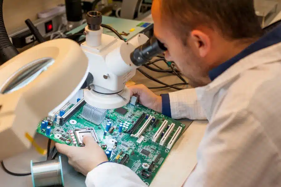
Final Visual Inspection (FVI) provides another quality checkpoint before shipment.
Operators may verify:
- Component orientation
- Solder joint appearance
- Connector condition
- PCB surface condition
- Labels and serial numbers
- Foreign material
- Mechanical damage
- Assembly completeness
Final inspection complements automated inspection by allowing trained personnel to evaluate conditions that may not be fully captured by automated systems.
Packaging
Correct packaging is essential because PCB assemblies can be damaged by electrostatic discharge, moisture, vibration, and mechanical shock during transportation.
Typical packaging materials include:
| Packaging Method | Main Purpose |
|---|---|
| ESD-safe bags | Prevent electrostatic damage |
| Moisture barrier bags | Reduce moisture exposure |
| Desiccant | Control internal humidity |
| Humidity indicator card | Monitor moisture conditions |
| Anti-static trays or foam | Prevent movement and mechanical damage |
| Reinforced cartons | Protect assemblies during transportation |
For prototype PCB assembly and small-batch orders, packaging can be optimized for flexibility and cost.
For high-volume or moisture-sensitive products, packaging requirements can be defined according to component MSL requirements, transportation conditions, storage duration, and customer specifications.
Kingda Advantage
Kingda provides controlled final inspection and packaging solutions according to customer requirements.
For products requiring enhanced traceability, labeling, ESD protection, moisture control, or customized packaging, these requirements can be incorporated into the manufacturing plan before production begins.
Step 10: Functional Testing and Continuous Improvement
Visual inspection alone cannot prove that a PCB assembly functions correctly.
Functional testing evaluates whether the assembled circuit operates according to its intended electrical and functional specifications.
Depending on the product, testing may include:
| Test Type | Function | Typical Application |
|---|---|---|
| Flying Probe Test | Checks electrical connections without a dedicated fixture | Prototypes and low-volume production |
| ICT | Tests individual circuit nodes and components | Medium- and high-volume production |
| Boundary Scan / JTAG | Tests IC interconnections | Dense digital circuits |
| Functional Test | Verifies actual product operation | Production and end-of-line testing |
Flying Probe Testing
Flying probe testing uses movable probes to contact designated test points.
It is particularly useful for:
- PCB prototypes
- Engineering samples
- Low-volume production
- Frequently changing designs
- Complex PCB layouts
Because a dedicated fixture may not be required, flying probe testing can reduce initial tooling costs.
In-Circuit Testing
In-Circuit Test (ICT) uses a test fixture to access multiple circuit nodes and verify electrical characteristics.
ICT can be highly efficient for stable, repeatable production where the fixture cost can be distributed across a larger production volume.
Functional Testing
A functional test powers the assembled PCB and verifies whether the complete circuit performs its intended function.
Depending on the product, this may include:
- Voltage measurement
- Current measurement
- Communication testing
- Sensor testing
- Display testing
- Motor control
- Power output verification
- Signal transmission
- Firmware-related verification
Rework and Repair
If AOI, X-ray, electrical testing, or functional testing identifies a repairable defect, the board may enter a controlled PCB rework process.
Typical rework operations include:
- Removing defective SMT components
- Replacing damaged components
- Repairing solder joints
- Reworking THT connections
- Cleaning the affected area
- Re-inspecting the repaired board
- Re-testing the assembly
Because excessive thermal exposure can damage PCB pads, components, or laminate materials, rework should be performed using controlled procedures and qualified technicians.
The goal of an effective PCB assembly process, however, is not simply to improve rework capability. It is to prevent defects before they occur through effective DFM review, process control, SPI, AOI, X-ray, and testing.
Continuous Improvement and Feedback
The final stage of PCB assembly should not be considered the end of the manufacturing process.
Production data can provide valuable information for improving the next PCB revision.
For example:
| Production Finding | Possible Improvement |
|---|---|
| Repeated solder bridging | Optimize stencil aperture design |
| Component polarity errors | Improve silkscreen and assembly documentation |
| Excessive BGA voiding | Optimize reflow profile |
| Repeated placement deviation | Review component library and placement data |
| Functional test failures | Improve test coverage or PCB design |
| Repeated mechanical interference | Conduct additional DFM review |
A structured feedback loop allows manufacturing information to flow back into PCB design and engineering.
This is particularly valuable during new product introduction (NPI) and the transition from prototype to mass production.
Key Equipment Used in PCB Assembly
Professional PCB assembly manufacturing relies on coordinated equipment rather than a single machine.
A typical SMT and PCBA production line may include:
| Equipment | Main Function |
|---|---|
| SMT Stencil | Controls solder paste deposition |
| Solder Paste Printer | Applies solder paste to PCB pads |
| 3D SPI | Measures solder paste volume, height, and alignment |
| Pick-and-Place Machine | Automatically places components |
| Reflow Oven | Creates reliable SMT solder joints |
| Thermal Profiler | Verifies reflow temperature profiles |
| AOI System | Detects visible assembly defects |
| X-Ray Inspection System | Inspects hidden solder connections |
| Selective Soldering System | Solder THT components selectively |
| Cleaning System | Removes residues and contaminants |
| Flying Probe Tester | Performs electrical testing |
| ICT System | Performs in-circuit testing |
| Functional Test System | Verifies actual product operation |
The specific equipment configuration should be selected according to PCB size, component density, package types, production volume, product reliability requirements, and testing requirements.
Why Choose Kingda for PCB Assembly?
As an experienced PCB manufacturer and PCB assembly service provider, Kingda provides integrated manufacturing support designed to help customers move from PCB design verification to production.
1. PCB Manufacturing and PCB Assembly Integration
By combining PCB manufacturing and PCB assembly services, Kingda can help reduce communication gaps between PCB fabrication and assembly.
This integrated workflow supports:
PCB Design → DFM Review → PCB Prototype → PCB Fabrication → PCB Assembly → Inspection → Testing → Production
Customers can work with a coordinated manufacturing partner rather than managing every stage independently.
2. Prototype to Volume Production
Different product development stages require different manufacturing strategies.
Kingda supports customers from:
- PCB prototypes
- Quick-turn PCB prototypes
- Engineering samples
- Low-volume PCB assembly
- Small-batch production
- Medium-volume production
- High-volume manufacturing
This makes it easier to transition a validated design into repeat production.
3. Engineering and DFM Support
Manufacturing problems are often easier and less expensive to solve before production begins.
Kingda can support DFM engineering review by evaluating factors such as:
- PCB layout manufacturability
- Component availability
- Pad design
- Component spacing
- Stencil requirements
- Assembly orientation
- SMT/THT process compatibility
- Testing requirements
The objective is to identify potential manufacturing risks before they become production problems.
4. Process-Based Quality Control
Kingda’s PCB assembly approach emphasizes process control rather than relying exclusively on final inspection.
Quality checkpoints can be integrated throughout the production workflow, including:
SPI → Placement Verification → Reflow Control → AOI → X-Ray → Electrical Testing → Final Inspection
This helps identify defects earlier and supports consistent production quality.
5. Support for Complex PCB Assemblies
Modern electronics increasingly require high-density and mixed-technology assemblies.
Kingda can support PCB assembly projects involving:
- Fine-pitch components
- BGA packages
- QFN/LGA packages
- High-density SMT
- Mixed SMT and THT assembly
- Double-sided PCB assembly
- Complex industrial electronics
- Automotive electronics
- Medical electronics
- Power electronics
- Communication equipment
The manufacturing process can be adapted according to product-specific requirements.
6. Traceability and Quality Documentation
For demanding applications, traceability is an important part of manufacturing quality.
Depending on project requirements, production documentation may include:
- Inspection records
- Test results
- Reflow profiles
- First-article inspection information
- Component information
- Production records
- Quality reports
- Corrective-action records
This provides customers with greater visibility into the manufacturing process.
PCB Assembly Process Flow
The complete PCB assembly workflow can be summarized as:
PCB Design → DFM Engineering Review → PCB Prototype Manufacturing → SMT Stencil → Solder Paste Printing → SPI Inspection → Component Placement → Reflow Soldering → AOI Inspection → SPC Process Control → X-Ray Inspection → THT/Selective Soldering → Cleaning → Functional Testing → Final Inspection → Packaging → Small-Batch Production → Volume Manufacturing
A well-designed process ensures that quality is controlled at every stage rather than inspected only at the end.
Conclusion
The PCB assembly process involves much more than simply placing components onto a circuit board. Each stage—from SMT stencil fabrication and solder paste printing to component placement, reflow soldering, AOI, X-ray inspection, selective soldering, and functional testing—contributes to the final quality and reliability of the PCBA.
For prototypes, the priority is usually rapid development, engineering flexibility, and design verification. For high-volume production, process stability, automation, traceability, yield, and cost control become increasingly important.
Choosing an experienced PCB assembly manufacturer can help reduce manufacturing risks and create a smoother path from prototype to mass production.
With professional PCB manufacturing, PCB assembly, DFM engineering, inspection, testing, and production support, Kingda helps customers turn PCB designs into reliable electronic assemblies and provides manufacturing solutions from initial prototype development through volume production.