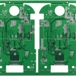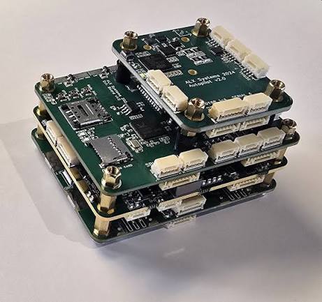
In the development of portable life-monitoring equipment, one of the most common engineering challenges is preventing wireless communication circuits from interfering with low-level physiological signal acquisition.
Bluetooth and Wi-Fi modules generate high-frequency RF energy during transmission. If the RF energy couples into sensitive ECG, SpO₂, or other analog acquisition circuits, it can introduce spikes, baseline disturbance, waveform distortion, or elevated noise levels.
In many projects, the schematic, sensor selection, and signal-processing architecture are technically sound, but an inappropriate PCB layout creates unexpected electromagnetic coupling. The resulting EMC problems may prevent the completed medical device from passing required compliance testing and can delay subsequent product qualification and registration activities.
This case describes how a carefully planned 4-layer PCB layout, functional zoning, power filtering, and return-path control can significantly reduce RF interference without increasing the number of PCB layers.
Project Requirements and RF Noise Symptoms
The customer developed a portable multi-parameter monitoring board capable of collecting ECG and blood oxygen signals. An MCU processed the acquired data, while a Bluetooth module transmitted the information to a mobile terminal.
The first prototype used a four-layer structure and initially passed basic functional testing. However, a typical interference problem appeared when the wireless module was activated.
When Bluetooth transmission was disabled, the ECG waveform remained relatively clean. Once Bluetooth transmission started, large amounts of high-frequency spikes appeared on the ECG waveform. The correlation between RF activity and signal degradation strongly suggested an electromagnetic coupling problem rather than a basic sensor or firmware malfunction.
The preliminary analysis identified two major potential coupling mechanisms:
- RF energy coupling through physical space
- RF current fluctuations propagating through the power distribution network
The board had several additional constraints:
- Limited PCB dimensions
- Four-layer construction
- Sensitive analog acquisition circuitry
- Digital MCU and memory
- Bluetooth RF circuitry and antenna
- Lithium-battery charging and protection circuits
- All functions had to remain on the same PCB
- No additional PCB layers could be added
The engineering objective was therefore to improve signal integrity through layout optimization and interference-control techniques while maintaining the existing four-layer structure.
Functional Zoning for a Medical 4-Layer PCB
The first major improvement was to divide the board into clearly defined functional areas.
For a medical PCB, functional zoning is more than simply placing similar components together. The physical location of each circuit determines how easily noise can couple into sensitive circuitry and how return currents travel through the board.
The design was divided into four primary zones:
Analog Acquisition Area
The analog front end included:
- Electrode input connectors
- Instrumentation amplifiers
- Reference circuits
- Analog filters
- Other high-impedance signal-conditioning components
This area was positioned near the external electrode interface and as far as practical from the Bluetooth antenna and RF circuitry.
The objective was to minimize the physical distance that extremely low-level analog signals needed to travel before amplification and filtering.
The analog input traces were kept within the analog area and were not routed through the digital or RF sections.
Digital Processing Area
The MCU, memory, clock circuitry, and related digital components were placed in a central region.
This area was separated from the sensitive analog input section to reduce the possibility of digital switching currents coupling into the analog front end.
Clock traces and other high-edge-rate signals were kept as short as practical and routed with controlled return paths.
RF and Bluetooth Area
The Bluetooth module, RF matching components, and antenna were placed on the opposite side of the board from the analog acquisition circuitry.
The antenna was positioned near the PCB edge, following the antenna manufacturer’s layout recommendations and keeping surrounding copper and components within the required antenna keep-out region.
This arrangement helps prevent the RF energy source from being unnecessarily close to the high-impedance analog inputs.
Power Management Area
The battery protection, charging circuitry, regulators, and related power components were grouped near the power-entry section.
This prevents high-current charging or switching currents from traveling through the sensitive analog area.
The fundamental zoning rule was simple:
Sensitive analog traces should not cross RF or high-speed digital regions, and RF antenna structures should not share unnecessary copper or return-current paths with the analog front end.
Power Distribution and Ground Return Control
Functional zoning alone cannot solve every interference problem. The power distribution and return-current paths must also be considered.
The board used a continuous internal ground plane rather than creating arbitrary ground-plane splits. For a compact four-layer design, maintaining a continuous reference plane can provide a predictable low-impedance return path when the stackup and routing are properly designed.
The power architecture was separated into functional branches:
- A dedicated regulated supply for the analog front end
- A separate regulated supply for digital circuitry
- An RF supply branch with additional filtering
- Power branches converging at an appropriate point near the battery-input side
The analog supply was routed directly toward the analog section without passing through high-current digital regions.
This approach helps prevent voltage fluctuations generated by digital or RF circuits from directly modulating the analog supply.
RF Power Filtering and Local Decoupling
RF transmission can produce rapid current variations. If these current fluctuations propagate through the power network, they can become another coupling mechanism.
An LC filtering network was therefore added to the RF power branch to attenuate unwanted high-frequency noise.
The analog front end also received dedicated local decoupling.
For example, a 0.1 μF capacitor may be placed close to an amplifier power pin when appropriate for the device and power architecture. The purpose is not simply to “add a capacitor,” but to minimize the effective high-frequency current-loop area and reduce local power impedance.
Component selection should be based on the IC manufacturer’s recommendations, operating frequency, package parasitics, DC bias characteristics, and the actual power-distribution network.
Additional bulk capacitance may also be required where load transients or regulator stability considerations justify it.
Trace Routing and Return-Path Management
Routing strategy was another major part of the PCB layout optimization.
Sensitive ECG and SpO₂ acquisition traces were kept on the appropriate signal layer and routed away from the RF section.
High-speed digital and RF-related traces were kept as short as practical, with their reference plane directly underneath or otherwise arranged to provide a controlled return path.
The key objective is to avoid forcing high-frequency return currents to travel through areas occupied by sensitive analog circuitry.
A signal trace and its return path should always be considered as one electromagnetic structure. Simply moving a signal trace away from another circuit does not guarantee adequate isolation if the associated return current is forced through a shared or sensitive region.
For RF transmission lines, the controlled-impedance geometry should follow the RF module or antenna manufacturer’s requirements. Unnecessary vias, abrupt geometry changes, and discontinuities should be minimized.
Protecting the Analog Front End
The analog front end is generally one of the most sensitive portions of a life-monitoring board.
Before amplification, ECG signals can be extremely small compared with the RF energy generated by a nearby wireless transmitter. The first-stage amplifier and input network therefore deserve special attention.
Important layout practices include:
- Keep sensor input traces short.
- Avoid routing them alongside RF transmission lines.
- Keep them away from fast digital clocks.
- Minimize unnecessary vias on high-impedance inputs.
- Place input filtering close to the relevant IC or connector.
- Maintain a stable reference environment.
- Avoid unnecessary copper structures around high-impedance nodes.
- Keep return-current paths predictable.
The analog front end should be treated as a protected functional region rather than simply another group of components on the PCB.
Controlling RF Coupling and EMI
RF interference can reach a sensitive circuit through several paths:
- Electric-field coupling between nearby conductors.
- Magnetic-field coupling caused by changing current loops.
- Conducted coupling through shared power networks.
- Common-impedance coupling through shared return paths.
- Radiated coupling from antennas, cables, connectors, or other structures.
Consequently, EMI control requires more than adding a filter after the problem occurs.
A useful engineering approach is to control the noise source, coupling path, and victim circuit simultaneously.
For the RF source, minimize unnecessary current-loop area and follow the module vendor’s RF layout requirements.
For the coupling path, increase physical separation, control reference planes, reduce parallel routing, and filter susceptible power branches.
For the victim circuit, minimize high-impedance exposed routing and provide appropriate filtering and shielding where necessary.
This source-path-victim approach is generally more effective than relying on a single mitigation measure.
Why Ground-Plane Splitting Is Not Always the Solution
A common response to mixed-signal interference is to divide the ground plane into separate analog, digital, and RF sections.
However, blindly splitting a ground plane can create discontinuities in return paths. High-frequency currents may then be forced to detour around the split, increasing loop area and potentially creating additional electromagnetic coupling.
For a compact 4-layer PCB, a continuous ground reference is often preferable when it can be combined with sensible physical zoning and routing.
The important distinction is between functional zoning and arbitrary copper-plane separation.
The circuits can be physically separated while still using a well-controlled common reference plane. Where actual ground separation is required by the system architecture, the connection strategy should be deliberately designed rather than implemented as a simple split under sensitive traces.
Antenna Placement and Keep-Out Requirements
The Bluetooth antenna is one of the strongest RF sources on the board.
Its position should be determined according to the antenna design, module documentation, enclosure constraints, and certification requirements.
In general, the antenna should be placed near a board edge with the manufacturer’s specified keep-out region respected.
Important considerations include:
- Keep sensitive analog inputs away from the antenna.
- Avoid placing large copper structures inside the antenna keep-out area.
- Follow the recommended ground and clearance configuration.
- Keep metal components away from the antenna where required.
- Avoid routing sensitive traces underneath the antenna region.
- Consider the influence of the enclosure, battery, display, cables, and connectors.
Antenna performance is highly dependent on its surrounding electromagnetic environment, so the final layout should be validated using the actual mechanical assembly rather than only the bare PCB.
Verification After Layout Optimization
After the layout was redesigned, the revised prototype was evaluated with Bluetooth transmission enabled.
The ECG waveform showed a significant reduction in the previously observed RF-related spikes, and the wireless communication function remained operational.
Subsequent EMC evaluation also showed improved radiated-emission performance, allowing the design to proceed through the required verification stage.
The exact test results and acceptance limits depend on the applicable product standards, test configuration, operating modes, enclosure, cables, and regulatory requirements. Therefore, the results from one project should be regarded as project-specific rather than universal performance benchmarks.
The most important engineering change was not a single filter component. It was the combined optimization of physical zoning, routing, power distribution, return paths, and antenna placement.
Practical Design Workflow for RF-Sensitive Medical PCBs
For similar projects, a structured workflow can help identify interference risks earlier.
Step 1: Classify Circuit Functions
Separate the PCB into:
- Sensitive analog circuits
- Digital processing circuits
- RF circuits
- Power conversion circuits
- High-current circuits
- External interfaces
Step 2: Identify Noise Sources
Determine which circuits generate the largest voltage or current transitions.
Typical sources include:
- RF transmitters
- Clock generators
- DC/DC converters
- PWM circuits
- High-speed digital interfaces
- Battery charging circuits
Step 3: Identify Sensitive Victims
Mark circuits that are particularly susceptible to interference.
Examples include:
- ECG inputs
- SpO₂ analog front ends
- Precision references
- High-impedance sensor inputs
- Low-level instrumentation amplifiers
- ADC inputs
Step 4: Define Physical Separation
Place high-noise sources away from sensitive circuits before detailed routing begins.
This is often more effective than trying to repair coupling problems after the placement has already been finalized.
Step 5: Design the Return Paths
Check where high-frequency currents will actually flow through the ground plane.
Do not evaluate signal traces independently from their return paths.
Step 6: Optimize Power Distribution
Separate sensitive analog supply branches from noisy switching or RF power paths where appropriate.
Use local decoupling and filtering based on the actual circuit requirements.
Step 7: Perform EMC-Oriented Verification
Evaluate the board in realistic operating modes, including wireless transmission, maximum digital activity, charging conditions, and other relevant worst-case states.
This is important because a board may appear quiet when the RF transmitter is inactive but exhibit interference under actual operating conditions.
Kingda’s Approach to High-Reliability Medical PCB Manufacturing
For a medical PCB, PCB fabrication and layout engineering cannot be considered completely independent.
A manufacturer involved early in the development process can help identify manufacturability constraints that may affect signal integrity, such as layer registration, controlled impedance, material selection, trace geometry, via structures, copper distribution, and stackup consistency.
Kingda can support medical and high-reliability PCB projects by working with engineering teams during prototype development and manufacturing preparation.
For RF-sensitive life-monitoring boards, the manufacturing review can include:
- Four-layer stackup verification
- Controlled-impedance requirements
- Fine-line fabrication capability
- Via and hole-position control
- Layer-registration requirements
- Copper distribution
- Solder mask considerations
- Material and dielectric selection
- Manufacturing consistency
- Prototype-to-production transition
A robust manufacturing process cannot replace good circuit design, but close communication between the designer and PCB manufacturer can reduce avoidable manufacturing variation and help preserve the intended electrical characteristics of the design.
Conclusion
For portable life-monitoring equipment, RF interference is often a system-level PCB design problem rather than a problem that can be solved by adding one filter component.
A wireless module can act as a strong noise source, while the ECG and SpO₂ acquisition circuits behave as highly sensitive victims. If these circuits are placed too close together or share unfavorable routing and return-current paths, RF energy can enter the analog acquisition chain and degrade the measured waveform.
The case demonstrates that effective EMI control can be achieved through coordinated physical zoning, power filtering, return-path management, antenna placement, and sensitive-signal routing.
For a compact 4-layer PCB, a carefully designed continuous reference plane combined with functional separation can provide an effective foundation for controlling interference.
Most importantly, the PCB layout should be considered part of the EMC design from the beginning. Early analysis of noise sources, coupling paths, and sensitive circuits can reduce debugging time and improve the reliability of medical monitoring products before they reach formal EMC and product qualification stages.
Kingda can support engineering teams in developing and manufacturing high-reliability PCBs for medical monitoring, wireless communication, and other applications where signal integrity and electromagnetic compatibility are critical.