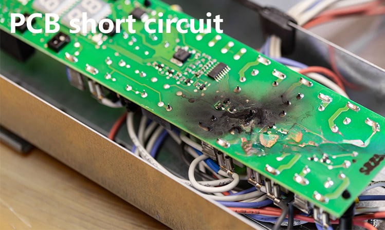
4-Layer RF PCB Cost: Materials, Stackup and Volume
Four layers is the most common stackup for RF work in the low gigahertz range, because it is the smallest construction that gives a microstrip line on the top layer, a solid reference immediately below it, and two more layers for power and control. This guide explains how a 4-layer RF PCB cost is built in 2025, where the money goes and which specification choices can be relaxed without damaging performance.
Why Four Layers Is the Common Starting Point
A two-layer RF board is possible, and it is used in simple products, but the reference plane has to share the bottom layer with routing, so every crossing breaks the return path. The result is unpredictable impedance and radiated energy that a shield may not fix. A four-layer board separates the reference from the routing and removes that problem at a modest cost increase.
The arrangement is normally a microstrip on the top layer, a ground plane immediately underneath, a power plane below that, and a mixed signal layer at the bottom. That gives the RF trace a defined reference, keeps the supply impedance low and provides two layers for everything that is not RF.
Stackup Choices and Their Cost
The stackup is where the cost is decided, because the dielectric thickness under the RF trace has to produce the required impedance. A thin dielectric between layer one and two gives a narrow trace and a tight field, which is good for isolation but more sensitive to etching tolerance. A thicker dielectric needs a wider trace and allows a looser process.
Material thickness also affects the mechanical construction. A thin core between the RF layer and its reference is easier to hold than a thick one, but a symmetric stackup is better for warping. Balancing those two requirements, and keeping the finished thickness standard, is what keeps the board on a proven process rather than a special one.

Materials: FR-4, Modified Epoxy and PTFE
Standard FR-4 works at low frequencies and in short runs, and its cost advantage is real. Above a few gigahertz its loss tangent becomes the limiting factor, and the variation of dielectric constant with frequency makes the impedance harder to hold. At that point a modified epoxy or a low-loss laminate becomes the practical requirement rather than a preference.
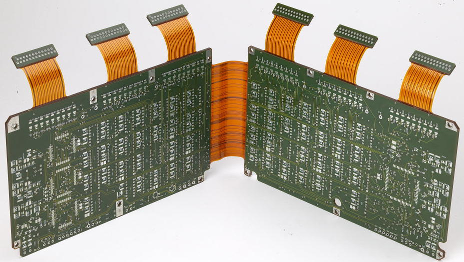
The step to a low-loss laminate is the largest single cost increase on the board, because the resin chemistry rather than the glass fabric dominates the price. A common compromise is a hybrid stackup, with the RF layers on the low-loss material and the other two layers on FR-4, bonded together in one lamination cycle.
Controlled Impedance and Test Coupons
Controlled impedance is charged as an engineering task plus a test coupon. The coupon is a strip of the same stackup included on the panel, measured to confirm that the dielectric thickness and the trace width produced the target impedance. That measurement is the evidence a customer needs, and generating it is real work.
The tolerance is the cost driver within that line item. A five percent impedance tolerance requires a tighter dielectric specification and more process control than a ten percent tolerance, and the price reflects it. Where a line feeds a matched component, the tighter figure is often worth paying for; where it feeds a short trace into a pad, it usually is not.
Vias, Stubs and Grounding
A via through a four-layer board from the top layer to the bottom creates a stub below the point where the trace leaves it, and that stub behaves as a resonator at high frequency. On a 4-layer board the effect is modest below a few gigahertz, but it grows quickly, and it is the reason back-drilling is specified on thicker constructions.
The cheaper mitigation is to plan the layer transitions. Keeping an RF trace on the top layer, using the bottom layer for baseband and control, and grounding the reference plane with a stitching via fence beside every RF line all reduce the problem. Applying microstrip and stripline routing rules is what makes the four-layer construction work without special processing.
Prototype versus Volume Pricing
The pcb prototype cost of an RF board includes the impedance coupon, the microsection and often a first-article report, so it is higher per unit than a digital board of the same size. On a small order those charges dominate, and they should be treated as the cost of evidence rather than as the cost of the product.
Volume pricing then depends on how much of the stackup is special. A hybrid stackup with a standard outer material and a low-loss inner pair is easier to scale than a fully low-loss construction, because the material is more widely stocked and the lamination window is wider. Standardising the stackup across several products is the largest single saving available at this layer count.
Regional Pricing and Hidden Costs
RF work is more sensitive to supplier capability than to region, because not every line can hold a tight dielectric tolerance or measure a coupon accurately. A cheaper quotation from a supplier without that capability is not a saving; it is an untested assumption in the design. Capability should be qualified before price is compared.
Hidden costs include the coupon, the microsection, the impedance report and any rework of the stackup needed to hit the target. Applying high frequency trace and reference plane rules from the first layout review is the cheapest way to avoid a stackup iteration, which would repeat all of those charges.
Reducing Cost Without Losing RF Performance
Restraint is the main lever. Use the low-loss material only where the loss budget requires it, keep the RF section as small as the function allows, avoid unnecessary layer transitions and stay with a standard finished thickness. Each of those decisions removes a special process rather than a capability.
What should not be reduced is the reference plane under the RF trace, the stitching via fence beside it or the impedance tolerance on a line that feeds a matched network. Those three items define whether the board works, and they cost very little compared with the cost of a redesign after the first measurement.
Additional Considerations for This Build
Practical attention to via stub pays for itself here, because it is one of the items that decides whether the finished board behaves as the drawing intended. Where the requirement is not stated on the fabrication drawing or in the assembly notes, the shop has to assume a default, and that default is rarely the value the design was simulated with. Stating via stub explicitly, together with the tolerance that applies, removes the assumption and keeps the result predictable from batch to batch.
Related reading: our fabrication notes, board quality and design release notes cover the same ground.
FAQ
Can a 4-layer board handle 5 GHz? Yes, with a suitable laminate and a controlled stackup. The limit is set by the loss budget and the impedance tolerance rather than by the layer count, and a hybrid stackup is often the most economical way to reach that frequency.
Do I need back-drilling on four layers? Usually not. The stub is short enough that its effect is modest at typical frequencies. Back-drilling becomes relevant on thicker boards or when the line must carry a very wide band.
Is a fully low-loss stackup necessary? Rarely. Most designs place only the RF layers on the low-loss material and use FR-4 for the power and control layers, which controls both the material cost and the lamination risk.