6-Layer PCB Prototype Guide: Process, Cost and Design Tips
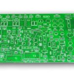
A 6-layer PCB prototype is a small batch of six-layer circuit boards made to validate a design before volume production. Product development teams use prototypes to test electrical behavior, fit, signal quality, and manufacturability. A 6-layer board provides more routing area, stable power and ground planes, and better signal integrity than a two-layer or four-layer board, making it common in communication, industrial, and consumer electronics.
Prototyping is an important step because it allows engineers to find design problems before investing in expensive tooling and large production runs. The sample board can be tested with real components and then revised if necessary. Understanding the manufacturing process and cost factors helps teams plan an efficient prototype program.
What Is a 6-Layer PCB?
A 6-layer PCB has six copper layers separated by insulating material. The stackup usually includes signal layers, power layers, and ground layers. The extra layers allow more components and traces to fit in the same area while improving electrical performance.
Compared with a two-layer board, a 6-layer board can separate sensitive signals from noisy power circuits. The power and ground planes provide low-impedance paths and reduce electromagnetic interference. The board is also better suited to high-speed interfaces that need controlled impedance.
A 6-layer stackup does not automatically make every design better. The layer arrangement must be planned carefully. If the stackup is unbalanced or the wrong layers are used, the board may have more problems than a simpler design.
Why Prototype a 6-Layer Board
A prototype gives engineers an actual board to test instead of relying only on simulation. Components can be placed, firmware can be loaded, and the complete system can be measured. This reveals issues that are difficult to predict from a schematic or layout review.
Signal integrity is often tested during prototyping. The engineer can use an oscilloscope or network analyzer to check impedance, crosstalk, and signal quality. Thermal behavior can also be measured by running the board at its expected load.
Prototyping also validates the manufacturing files. Gerber files, drill files, stackup information, and special process notes are checked against the real board. This reduces the risk of discovering a problem during volume production.
Designing the 6-Layer Stackup
The stackup of a 6-layer PCB should be chosen before routing begins. A common arrangement places signal layers near ground planes so that return currents flow directly beneath the signal path. Power and ground planes should be close together to create good high-frequency decoupling.
Layer thickness and dielectric material affect impedance. The manufacturer can provide a controlled impedance stackup when the design has high-speed nets. Trace width is calculated from the target impedance, copper weight, and dielectric spacing.
The stackup should also be balanced to reduce warpage. Thick copper layers, solder mask, and silkscreen can create stress if the board is not symmetrical. A balanced construction is easier to assemble and less likely to bend.
Signal Integrity and EMI Control
Six-layer boards are often used for high-speed circuits because they can provide clean reference planes. High-speed traces should be routed over a continuous ground plane. Avoid cutting the plane with long slots or routing too close to the edge.
Separate digital and analog circuits when possible. Keep clock and data lines away from sensitive analog inputs. Add filtering near connectors and place decoupling capacitors close to power pins.
Electromagnetic compatibility depends on more than the PCB, but a good layout makes the product easier to shield. Short return paths, minimal loop area, and proper grounding reduce emissions and improve immunity.
Manufacturing Process for 6-Layer Prototypes
A 6-layer PCB prototype is made by laminating multiple inner layers together. The process begins with inner-layer imaging and etching. Each layer is inspected before lamination so that defects are not hidden inside the board.
The inner layers are aligned with prepreg and pressed under heat and pressure. After lamination, holes are drilled according to the drill file. Plated through holes connect the layers, and outer-layer imaging creates the final copper pattern.
Solder mask is applied to protect the copper and prevent solder bridges. Silkscreen adds component markings. The surface finish is applied last to protect exposed pads and improve solderability.
Blind and Buried Vias in Prototypes
Some 6-layer designs use only through vias, which is simpler and more economical. Others need blind vias or buried vias to improve routing density. Blind vias connect an outer layer to an inner layer, while buried vias connect internal layers only.
Special via structures require additional process steps and increase prototype cost. They should be used only when needed. In a 6-layer board, buried vias can reduce the number of through holes and improve routing in dense areas.
Via-in-pad may also be used for small-pitch components. The via is placed directly in the component pad and filled or capped so that solder does not disappear into the hole. This creates a compact layout but must be specified clearly in the manufacturing file.
Quality Testing for Prototype Boards
A reliable 6-layer PCB prototype should be tested before delivery. Visual inspection checks solder mask, silkscreen, and surface finish. Automated optical inspection can find etching defects and missing features.
Electrical testing verifies continuity and isolation. A flying probe tester checks opens and shorts without requiring a fixture, which is convenient for prototypes. Impedance testing confirms that high-speed traces meet the specified target.
The customer should also perform functional testing after assembly. Measure power, clock, communication, and input/output behavior under real operating conditions. Any failure should be traced back to the layout, stackup, material, or assembly process.
Surface Finish and Special Processes
Surface finish is selected according to the assembly process and environment. ENIG is common for boards with fine-pitch components because it provides a flat, solderable surface. OSP is economical for some lead-free processes, while immersion silver and hard gold are used for other applications.
The prototype should use the same finish planned for volume production. If the finish changes later, solderability and assembly results may also change. This is especially important when the board is tested with real components.
Special requirements such as impedance coupons, edge plating, castellated holes, or conformal coating should be documented in the prototype order. The manufacturer should confirm that it can support these features before fabrication begins.
Prototype Lead Time and Cost
Lead time for a 6-layer PCB prototype depends on layer count, material availability, special processes, and the factory’s production schedule. Standard 6-layer boards can often be delivered more quickly than boards with blind, buried, or high-frequency features.
Cost is driven by board size, layer count, material, copper weight, hole count, surface finish, and quantity. Prototype pricing usually includes engineering setup, so ordering several small revisions at the same time may be more efficient than placing many one-off orders.
The team should define realistic delivery expectations. A quick-turn prototype may cost more, while a standard lead time may give the factory enough time to control quality. The best choice depends on the project schedule and development stage.
Design for Manufacturing Checklist
Before sending a 6-layer PCB for prototyping, check trace width and spacing against the supplier’s capability. Verify hole size, annular ring, and board thickness tolerances. Ensure the stackup is balanced and controlled impedance values are clear.
Use a reasonable number of different drill sizes. Every unique drill size adds setup time and cost. Panelize the board if multiple units are needed, but leave enough space for routing and fiducials.
Document special instructions in the fabrication drawing. Include copper weight, surface finish, solder mask color, silkscreen, impedance requirements, and test method. Clear communication reduces the risk of manufacturing errors.
Applications of 6-Layer PCB Prototypes
Communication equipment such as 5G routers, switches, and radio modules uses 6-layer PCBs for high-speed signal processing. The prototype helps engineers verify impedance and high-frequency performance before production.
Industrial automation uses 6-layer boards in PLCs, servo drives, and control modules. These products need reliable boards that can operate in noisy factory environments. Prototypes allow the team to test communication, power, and electromagnetic behavior.
Consumer products such as smartphones, tablets, smart watches, and home appliances also use 6-layer boards when they need more integration and better signal quality. A prototype makes it possible to check size, function, and performance before the final product is built.
Choosing a Prototype Supplier
A good 6-layer PCB prototype supplier should be able to review design files and provide practical feedback. Ask about layer count capability, minimum trace width, drill size, controlled impedance, and delivery time. The supplier should also explain how it tests prototype boards.
PCB design and layout support can help optimize the stackup before fabrication. Once the files are ready, PCB manufacturing should produce the prototype with the same process discipline used for volume boards.
After the bare board is tested, prototype PCB assembly can place components and verify the complete module. If additional revisions are needed, the team can repeat the process quickly. For final production, turnkey PCB assembly and component procurement provide a smooth transition.
Conclusion
A 6-layer PCB prototype is a practical way to validate a multilayer design before committing to high-volume production. It helps engineers test signal integrity, fit, function, and manufacturability while avoiding the cost of large-scale errors.
By planning the stackup, documenting special requirements, and working with an experienced manufacturer, product teams can complete prototype testing quickly and move into production with confidence.