As electronic products become smaller, lighter, and more highly integrated, the requirements for printed circuit boards are becoming increasingly demanding. During the PCB Design and PCB Manufacturing processes, engineers need to consider not only electrical performance but also manufacturability, assembly requirements, thermal management, mechanical strength, and long-term reliability.
A small design error or process deviation can lead to serious problems such as short circuits, open circuits, soldering failures, component displacement, or premature product failure.
For this reason, identifying potential problems early in the design and manufacturing stages is essential for improving PCB Reliability and reducing production costs.
Kingda has summarized eight common PCB design and manufacturing problems, together with their major causes and recommended preventive measures.
1. PCB Short Circuits
A PCB Short Circuit is one of the most common PCB failures. It occurs when two conductive areas that should remain electrically isolated become unintentionally connected.
A short circuit may prevent the PCB from operating correctly and, in some cases, may cause excessive current, component damage, or permanent circuit failure.
Common Causes of PCB Short Circuits
Improper pad design:
Insufficient spacing between adjacent pads can increase the possibility of solder bridging during assembly. Pad dimensions should therefore be designed according to component specifications and the actual capabilities of the PCB manufacturing process.
For certain designs, an elongated or oval pad may provide greater clearance between adjacent conductive areas than a circular pad.
Incorrect component orientation:
Component orientation can have a significant effect on soldering quality. This is especially important for components with closely spaced leads during wave soldering.
For example, if a leaded component is positioned incorrectly relative to the direction of solder flow, molten solder may connect adjacent leads and create a short circuit.
Excessive or improperly formed component leads:
Component leads that are too long or excessively bent may come into contact with neighboring conductors or component leads.
The lead length and forming angle should therefore be controlled according to the assembly requirements.
Other possible causes include:
- Excessively large holes
- Insufficient soldering temperature
- Poor PCB surface solderability
- Damaged solder mask
- Contamination on the PCB surface
- Excessive solder paste
- Incorrect component placement
- Insufficient spacing between conductive traces
How to Prevent PCB Short Circuits
During PCB Design, engineers should carefully check trace spacing, pad clearance, solder mask openings, component orientation, and minimum electrical clearance.
During assembly, solder paste volume, stencil design, component placement accuracy, and reflow parameters should also be carefully controlled.
Automated optical inspection can further help identify solder bridges and other visible defects before the PCB is delivered.
2. Dark or Black Solder Joints and Particles
Dark or black areas around Solder Joints may indicate solder contamination, excessive oxidation, or inappropriate soldering conditions.
Oxides and impurities mixed into molten solder can negatively affect the appearance and mechanical properties of the solder joint.
However, a dark solder joint does not necessarily mean that low-tin solder has been used. The actual cause should be determined through material and process analysis.
Possible Causes
- Excessive oxidation of the solder
- Contaminated solder material
- Changes in solder alloy composition
- Excessive soldering temperature
- Improper thermal profile
- Contamination on the PCB surface
- Excessive thermal stress
If solder contamination is confirmed, the solder material should be inspected and replaced with qualified material when necessary.
The thermal profile should also be reviewed. Excessive preheating or soldering temperatures can cause thermal stress to the PCB substrate and may contribute to delamination or other material-related problems.
Recommended Solution
Kingda recommends controlling solder material quality, monitoring soldering temperature, and regularly checking the condition of soldering equipment.
For critical applications, solder joint cross-section analysis can be used to evaluate the internal structure and determine whether the joint meets the required quality standards.
3. Golden or Yellow Solder Joints
Most conventional solder joints have a silver-gray metallic appearance. However, solder joints may occasionally appear yellow or golden after soldering.
One possible cause is excessive temperature or prolonged exposure to high temperatures.
High temperatures can increase oxidation and may alter the appearance of the solder joint or PCB surface finish.
How to Prevent This Problem
Engineers should verify the soldering temperature profile and ensure that it matches the requirements of the solder alloy and PCB surface finish.
The following parameters should be monitored:
- Peak soldering temperature
- Heating rate
- Time above liquidus
- Cooling rate
- Conveyor speed
It is important to note that solder joint color alone should not be used as the only indicator of soldering quality. Electrical testing, visual inspection, microscopic inspection, and cross-sectional analysis may be required for critical applications.
4. Environmental Factors Affecting PCB Reliability
Environmental conditions can have a major impact on PCB Reliability.
Even when a PCB is correctly designed and manufactured, exposure to extreme temperatures, humidity, vibration, mechanical shock, dust, or excessive electrical stress may gradually reduce its performance.
Temperature and Thermal Cycling
Temperature changes cause PCB materials to expand and contract.
Because copper, resin, laminate materials, solder, and electronic components have different coefficients of thermal expansion, repeated thermal cycling can create mechanical stress.
Over time, this may result in:
- Solder joint fatigue
- PCB warpage
- Copper trace cracking
- Delamination
- Component damage
- Via reliability problems
Humidity and Corrosion
Moisture can accelerate oxidation and corrosion of exposed copper, pads, solder joints, and component leads.
For electronic products used in humid environments, engineers may need to consider conformal coating, appropriate surface finishes, sealing structures, or other moisture-protection methods.
Dust and Contamination
Dust and contaminants accumulated on the PCB surface may restrict airflow and reduce heat dissipation.
For high-power circuits, this can increase component operating temperatures and potentially shorten component life.
Vibration and Mechanical Shock
Vibration, impact, dropping, or repeated bending may deform the PCB and damage components or solder joints.
For products exposed to significant mechanical stress, PCB mounting structures and component reinforcement should be carefully designed.
Electrical Overstress
Excessive current can cause PCB traces to overheat, while excessive voltage can result in dielectric breakdown or component damage.
Therefore, trace width, copper thickness, creepage distance, clearance, thermal management, and circuit protection should all be considered during PCB Design.
5. PCB Open Circuits
A PCB Open Circuit occurs when an electrical path is unintentionally interrupted.
This can happen when a copper trace is broken or when a solder joint fails to establish a reliable connection between the component and PCB pad.
Common Causes
- Broken copper traces
- Insufficient solder
- Poor solder wetting
- Cracked solder joints
- Damaged component leads
- PCB bending
- Mechanical impact
- Corrosion
- Poor plating
- Delamination
- Manufacturing defects
Mechanical stress is a particularly important factor. Repeated bending, vibration, or impact may cause cracks in copper traces or solder joints.
Moisture and chemical contamination may also accelerate corrosion and gradually weaken conductive connections.
Prevention
During PCB Manufacturing, electrical continuity testing should be performed where appropriate.
Automated testing and visual inspection can help identify open circuits before the product reaches the final assembly stage.
For high-reliability products, additional electrical and structural testing may be required.
6. Loose or Misaligned PCB Components
During reflow soldering, components may move slightly while the solder paste is in a molten state.
This can result in component displacement, rotation, tilting, or poor alignment with the PCB pads.
Common Causes
Component movement may be caused by:
- Insufficient PCB support
- Uneven solder paste deposition
- Excessive solder paste
- Incorrect placement coordinates
- Poor PCB positioning
- Incorrect reflow temperature profile
- Mechanical vibration
- Component placement errors
For fine-pitch and high-density assemblies, even a small component displacement may cause solder bridges or electrical problems.
Prevention
Accurate placement programming, stable solder paste printing, proper PCB support, and optimized reflow parameters are essential.
AOI inspection should also be used to verify component position, orientation, and soldering quality after assembly.
7. Common Soldering Defects
Soldering Defects are another major source of PCB assembly failures. They can affect both electrical performance and the mechanical reliability of the assembled product.
Cold Solder Joints
A cold solder joint occurs when the solder does not melt or wet the surfaces properly.
The resulting joint may have a rough appearance and poor mechanical strength.
Possible causes include:
- Insufficient soldering temperature
- Insufficient heating time
- Contaminated surfaces
- Improper solder paste
- Poor thermal transfer
The affected joint should be reheated under controlled conditions, and excess or defective solder should be removed if necessary.
Solder Bridges
A solder bridge occurs when solder unintentionally connects two adjacent pads or component leads.
This creates an unwanted electrical connection and may result in a PCB Short Circuit.
Solder bridges are particularly common in fine-pitch components when stencil apertures, solder paste volume, or placement accuracy are not properly controlled.
Insufficient Solder
Insufficient solder may result in weak mechanical connections and unreliable electrical performance.
The problem may be caused by inadequate solder paste volume, incorrect stencil design, poor paste transfer, or inappropriate soldering conditions.
Excessive Solder
Excessive solder can cause solder bridges, uneven joints, component floating, and other assembly problems.
The solder paste printing process should therefore be carefully controlled.
Pad Lifting
Pad lifting occurs when a PCB pad partially or completely separates from the PCB substrate.
It may be caused by excessive heat, mechanical force, aggressive rework, or repeated soldering.
Appropriate temperature control and professional rework procedures can significantly reduce this risk.
8. Human Error and Process Control
Human error can contribute significantly to PCB manufacturing and assembly defects.
Incorrect production procedures, inaccurate component placement, insufficient process documentation, inadequate operator training, and poor inspection practices can all increase the defect rate.
As PCB complexity increases, manufacturing becomes more demanding because of:
- Higher component density
- More PCB layers
- Fine-pitch components
- Narrower trace widths
- Smaller vias
- Complex power and ground structures
- Surface-mount technology
- Multiple assembly processes
For this reason, manufacturers should establish standardized operating procedures and provide appropriate employee training.
Automated equipment and inspection systems can also reduce the risk associated with manual operations.
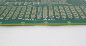
How to Improve PCB Manufacturing Quality
Preventing PCB defects should begin before production starts.
During PCB Design, engineers should consider:
- Trace width and spacing
- Pad dimensions
- Component placement
- Solder mask clearance
- Thermal management
- Mechanical strength
- Electrical clearance
- Manufacturing tolerances
- Assembly requirements
During PCB Manufacturing, process parameters should be continuously monitored and controlled.
During assembly, solder paste printing, component placement, reflow soldering, cleaning, and inspection should be managed as an integrated process rather than as independent steps.
For high-reliability applications, manufacturers can combine AOI, X-ray inspection, electrical testing, microscopic examination, and other quality-control methods.
Kingda applies standardized manufacturing and inspection procedures throughout PCB production and assembly. By combining engineering review, automated equipment, process monitoring, and professional quality control, Kingda works to minimize defects and improve overall PCB Reliability.
Conclusion
PCB problems can originate from many different sources, including design errors, material issues, manufacturing deviations, soldering conditions, environmental stress, and human error.
The most common problems include PCB Short Circuit, PCB Open Circuit, solder bridges, cold solder joints, component misalignment, corrosion, and mechanical damage.
The best way to reduce these problems is to identify potential risks early in the design stage and maintain strict process control throughout manufacturing and assembly.
A well-designed PCB, combined with stable manufacturing processes and comprehensive inspection, can significantly improve product reliability and reduce production costs.
Kingda is committed to providing professional PCB manufacturing and assembly solutions with a focus on quality, consistency, and long-term PCB Reliability. Through continuous process optimization and strict quality management, Kingda helps customers achieve reliable PCB products for a wide range of electronic applications.