What Is PCB Assembly? A Complete Guide
PCB assembly is the process of soldering electronic components onto a bare printed circuit board (PCB). Before taking a closer look at printed circuit board assembly, let’s first understand what a PCB is.
A PCB, or printed circuit board, is an electronic board on which components are attached or mounted to perform specific functions.
Components used in PCB assembly can generally be divided into passive components and active components. Passive components do not provide power gain to a circuit, while active components can amplify input signals.
Printed circuit board assembly can be performed manually or by machine. However, automated equipment is used in most applications because it provides higher efficiency, consistency, and reliability.
Generally, PCB assembly can be divided into two main types: through-hole technology (THT) and surface mount technology (SMT).
Two Main Types of PCB Assembly
The demand for smaller, lighter, and more durable electronic devices has driven continuous changes in PCB assembly processes.
Since printed circuit boards became commercially available in the 1950s, PCBA manufacturing has evolved into two major technologies: through-hole technology (THT) and surface mount technology (SMT). These are essential capabilities for professional PCB assembly manufacturers.
Through-Hole Technology (THT)
The older PCB assembly method involves inserting component leads through pre-drilled holes in the PCB to create interconnections between different layers. This method is known as through-hole technology (THT).
Components are typically inserted using an automatic insertion machine. The required program is first uploaded to the machine controller.
The PCB then goes through a wave soldering process, where it is conveyed over a molten solder wave and immersed for several seconds.
Two types of components can commonly be connected to a PCB using through-hole technology:
- Axial-lead components – leads extend along the component’s axis.
- Radial-lead components – leads extend perpendicular to the main axis of the electronic component.
After automatic insertion and wave soldering, the PCB undergoes electrical testing to identify open circuits and short circuits. This can be done by checking the resistance between circuit nodes when the board is powered.
Advantages of Through-Hole Technology
THT is a mature technology, but it remains widely used in many applications because of the following advantages:
High Mechanical Strength
With through-hole technology, component leads pass through the layers of the PCB and are securely soldered, providing strong mechanical connections. This makes THT particularly suitable for equipment exposed to frequent mechanical stress.
Easier Adjustment and Repair
Because THT components are inserted through the PCB and soldered on the opposite side, they are relatively easy to remove, adjust, and replace. This also makes THT convenient for testing and prototyping.
High Power Handling Capability
Through-hole components are generally larger than surface-mount components and can offer higher power-handling capabilities. THT is widely used for high-current applications involving transistors, transformers, regulators, and other power components.
Excellent Durability
The high mechanical strength of THT connections provides excellent durability, even under demanding environmental conditions. Their robust connections and larger physical size make them more resistant to vibration and thermal stress, helping extend product service life.
Surface Mount Technology (SMT)
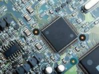
The more modern PCB assembly method uses solder paste to mount components directly onto pads on the surface of the circuit board.
This allows components to be placed with much smaller spacing.
The miniaturization of electronic devices has driven the widespread adoption of SMT because it supports smaller pads, smaller packages, and more compact circuit designs.
Although SMT offers significant advantages, some applications still require THT or a combination of SMT and THT.
Power electronics are one example, where components such as transformers and capacitors may require the mechanical strength provided by through-hole connections.
Advantages of Surface Mount Technology
SMT offers numerous advantages for producing smaller devices with greater functionality. Compared with THT, more PCB assembly manufacturers use SMT for modern electronic products.
Smaller and Lighter Packages
With SMT, components can be mounted directly onto the PCB with smaller spacing and finer leads. Unlike THT, no through-holes are required for component mounting. This enables smaller and lighter packages.
Higher Pin and Lead Counts
Surface mount technology allows more pins and leads to be installed on the PCB surface, enabling a higher number of input/output connections.
Greater Functionality
Because SMT supports higher pin and lead counts, more interconnections can be integrated into a smaller area, allowing greater functionality within a compact PCB design.
High-Frequency Operation
The higher component density enabled by SMT allows shorter electrical connection paths, making it suitable for high-frequency applications.
Basic PCB Assembly Process
1. Solder Paste Printing
Solder paste printing is the first step in the SMT PCB assembly process. A stencil printing process is used to deposit solder paste onto the PCB pads.
Most industries now use lead-free solder pastes, such as SAC solder paste, to comply with hazardous substance regulations.
SAC stands for an alloy of tin, silver, and copper.
During solder paste printing, a squeegee moves across a metal stencil containing solder paste and evenly distributes the paste through the stencil openings onto the PCB pads.
2. Component Placement
During component placement, an automatic pick-and-place machine picks up the required components and places them on the PCB according to predefined positions and orientations.
The tackiness of the solder paste temporarily holds the components in place during the PCB assembly process.
3. Reflow Soldering
The PCB with its components is transferred into a reflow oven. It is first preheated to a predetermined temperature below the peak temperature.
The preheating stage allows the flux to activate and provides controlled thermal treatment for the components.
The temperature then gradually increases until it reaches the peak temperature required to fully melt the solder paste.
After reaching the peak temperature, the temperature decreases to promote solder solidification and complete the soldering process. Heating can be achieved through infrared (IR) radiation or convection hot air.
4. Automated Optical Inspection (AOI)
Manual inspection is not always reliable because it can be affected by inconsistencies and differences in human judgment. Automated optical inspection (AOI) equipment is therefore used to provide faster and more consistent inspection.
AOI is an important additional inspection step in PCB assembly because not every defect can be detected through electrical testing.
5. PCBA Testing
In-circuit testing and flying probe testing are two common methods for detecting electrical faults after PCB assembly.
In-circuit testing (ICT) uses a fixture similar to a bed of nails, on which the circuit board is mounted for electrical testing.
Flying probe testing is a lower-cost but generally slower option that uses a set of movable probes to test the PCBA.
What Key Factors Should Be Considered in PCB Assembly?
Material Shortages
Material shortages in the electronics industry can be caused by many factors, including raw material availability, government regulations, aging or discontinued equipment, PCBA supplier factory closures, and relocation of production facilities.
An effective strategy is to include alternative components and/or alternative PCB assembly suppliers in your material shortage contingency plan.
China can be an attractive location for PCB assembly because of its extensive manufacturing infrastructure and supply chain resources.
Manufacturing and Quality Control
Because PCBs are highly specialized products with specific quality requirements, a comprehensive manufacturing control system is essential.
For example, the temperature during reflow soldering must remain within a specified range to prevent soldering defects. Some PCBA suppliers use reflow ovens with multiple heating zones to achieve more precise temperature control.
Capacity Improvement
Capacity improvement focuses on maximizing overall equipment effectiveness (OEE), maintaining machine flexibility, increasing throughput, and reducing setup and changeover times.
In PCB manufacturing, component placement is often a bottleneck. Therefore, optimizing the placement sequence and movement path for different components can significantly improve production efficiency.
Common PCB Assembly Defects and Solutions
Solder Bridging
The reflow soldering process can cause soldering defects such as solder bridging. Excessive solder paste or an incorrect temperature profile can cause solder to spread and connect with solder on adjacent pads.
This can result in electrical shorts and PCB assembly failures.
Solution: Determining the correct solder paste volume and optimizing the thermal profile can reduce the occurrence of solder bridges.
Component Misalignment
If components are improperly placed on the solder paste, or if the solder paste beneath a component is uneven, the component may shift during reflow.
This can result in component misalignment and lead to open or short circuits. As electronic components become smaller, accurate component alignment becomes increasingly important.
Solution: The solder paste must be evenly distributed across the pads. Proper programming of the pick-and-place machine is also essential to ensure accurate component placement.
Poor Solder Wetting
Sometimes, solder does not adequately wet the contact pads during soldering. This can occur when oxidation is present on the contact pads or conductive materials being joined.
Oxidation is common during heating, which is why introducing nitrogen into the reflow process can help reduce oxidation.
Solution: Proper cleaning is essential for maintaining good solder wetting. In PCB assembly, solder paste expiration dates, storage conditions, and shelf life should also be carefully controlled.
Tombstoning
Another common PCBA defect is tombstoning, where a component stands upright on one end because of an imbalance in soldering forces.
When the solder on both ends of a component does not melt or solidify at the same time, the uneven forces can cause the component to lift from one side.
Solution: The thermal profile should be optimized to achieve a uniform temperature distribution across the PCB.
The stencil aperture design should also be carefully evaluated to ensure balanced solder paste deposition on both sides of the component.
Why Choose Us as Your PCB Assembly Partner?
If you are looking for cost-effective PCB assembly services, choosing a China-based PCB assembly manufacturer can be a practical option.
China has a well-established electronics manufacturing ecosystem, extensive supply chain resources, skilled technical personnel, and mature production capabilities.
Viasion is recommended here as a China-based PCB assembly service provider with more than 16 years of experience.
Its capabilities cover product quality, competitive pricing, logistics, customer support, and technical expertise.
Here are several reasons to consider us as your PCB assembly partner.
Competitive Pricing
We provide an efficient quotation process to help you make informed decisions for your business. Our services and products are offered at competitive prices.
We work to establish clear and accurate requirements and expectations before confirming the final quotation, helping ensure transparency throughout the project.
High-Quality and Reliable Products
We manufacture high-quality PCB assemblies that are assembled and tested according to applicable specifications, international standards, and internal quality control requirements.
Before full-scale production, we follow a systematic product inspection process to verify the stability and reliability of the PCB assembly process.
Delivery and Lead Times
As an experienced PCB assembly manufacturer in China, we maintain our assembly equipment in optimal condition to maximize production efficiency and minimize downtime.
Our customers value our fast production and delivery cycles. We also provide expedited PCB assembly services when faster delivery is required, while maintaining consistent product quality.
Responsive Customer Support
We respond promptly to customer requirements and provide clear and accurate information to minimize misunderstandings.
Multiple communication channels are available to answer technical and project-related questions. We also provide one-stop PCB assembly services to simplify the entire procurement process.
Technical Capabilities
China has developed strong technical capabilities in PCB assembly and electronics manufacturing. We provide comprehensive SMT solutions covering PCB assembly, inspection, testing, and reliability verification.
We also offer prototyping services and customized PCB assembly solutions tailored to specific product requirements, helping customers move from prototype development to production more efficiently.