High-Quality Double-Sided PCBs at Competitive Prices
GOPCBA provides reliable Double-Sided PCB manufacturing solutions for electronic products ranging from prototypes to production applications. A two-layer PCB offers more routing space and circuit density than a single-sided board while maintaining a lower manufacturing cost and simpler structure than many multilayer designs.
Our PCB manufacturing capabilities support a wide range of materials and technical requirements, including FR-4, high-TG materials, high-frequency materials, aluminum, copper-based substrates, ceramic materials, PTFE and other specialty PCB materials. Our manufacturing capabilities also cover standard and advanced PCB technologies, with electrical testing and inspection integrated into the production process.
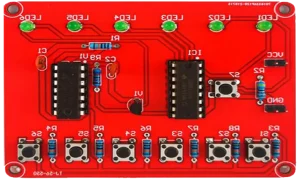
For projects that require both bare-board fabrication and component assembly, customers can also connect their PCB project with our PCB Assembly services for a streamlined manufacturing process.
What Is a Double-Sided PCB?
A Double-Sided PCB, also known as a two-layer PCB or 2-layer PCB, contains conductive copper layers on both the top and bottom sides of the board. These two copper layers are separated by an insulating dielectric substrate, such as FR-4.
Electrical connections between the top and bottom copper layers are commonly established through plated through-holes and vias. Components can also be mounted on either side of the board, allowing engineers to achieve a higher circuit density within a relatively compact PCB footprint.
Compared with single-sided PCBs, double-sided boards provide substantially more routing flexibility. Compared with multilayer PCBs, they generally offer a simpler manufacturing structure and lower overall cost.
For applications that require more complex routing, higher signal density, controlled impedance, or additional power and ground planes, a multilayer PCB may be a more suitable solution.
Main Components of a Double-Sided PCB
Copper Traces
Copper traces form the electrical pathways connecting components and circuit sections. In a double-sided PCB, routing can be distributed between the top and bottom copper layers, providing greater layout flexibility.
Trace width, spacing, current capacity, impedance, and copper thickness should be considered during PCB design. Proper routing is particularly important for power circuits, high-speed signals, and sensitive analog circuits.
Pads
Pads are conductive areas designed for component soldering and electrical connection. Their size, shape, spacing, and position must match the component package and assembly process.
Well-designed pads improve solderability, mechanical stability, and manufacturing consistency.
Plated Through-Holes and Vias
Plated through-holes provide electrical connections between the two copper layers. Depending on the design, vias can be used to transfer signals, ground connections, and power between the top and bottom layers.
Via diameter, annular ring, spacing, and placement should be considered carefully because they affect manufacturability, routing density, and electrical performance.
Solder Mask and Silkscreen
A solder mask protects exposed copper from oxidation and helps prevent accidental solder bridging during assembly. It is normally applied to both sides of the PCB.
The silkscreen layer is used to display component references, polarity indicators, logos, markings, and other assembly information.
Surface Finish
Exposed copper pads normally require a surface finish to improve oxidation resistance and solderability.
Common PCB surface finishes include:
- HASL
- Lead-Free HASL
- ENIG
- OSP
- Immersion Tin
- Immersion Silver
The appropriate finish depends on the application, component package, soldering process, reliability requirements, and cost target.
Advantages of Double-Sided PCBs
More Available Routing Space
Using both sides of the board provides significantly more routing space than a single-sided PCB. Components and traces can be distributed across the top and bottom surfaces to create a more compact design.
Higher Circuit Density
A 2-Layer PCB can accommodate more complex circuits than a single-sided board without the additional manufacturing complexity of a multilayer construction.
Flexible Component Placement
Components can be installed on either side of the board, giving engineers greater flexibility when optimizing circuit layout, mechanical dimensions, and assembly requirements.
Cost-Effective Manufacturing
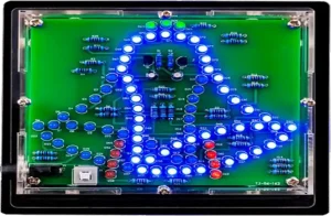
For many electronic products, double-sided PCB manufacturing provides a practical balance between circuit density and production cost. When a design does not require additional internal layers, a two-layer board can be more economical than a multilayer PCB.
Suitable for Prototypes and Production
Double-sided PCBs are widely used for prototypes, low-volume manufacturing, and production applications. GOPCBA supports PCB projects from prototyping through volume manufacturing, with engineering support and manufacturing process control.
Limitations of Double-Sided PCBs
Limited Routing Density
Although a double-sided PCB provides more routing space than a single-sided board, it still has only two conductive layers. Highly complex circuits may quickly exceed the available routing space.
More Difficult Signal Management
When a design contains high-speed digital signals, analog signals, RF signals, and multiple power domains, routing everything across two layers can become challenging.
Limited Power and Ground Plane Options
A two-layer structure provides less flexibility for dedicated power and ground planes than multilayer construction. Engineers must therefore pay greater attention to current paths, return paths, grounding, and electromagnetic compatibility.
Not Ideal for Highly Complex Designs
Dense BGA layouts, advanced high-speed interfaces, complex RF circuits, and designs requiring extensive impedance control may benefit from four-layer or higher-layer PCB construction.
GOPCBA’s PCB capabilities extend from standard boards to advanced multilayer, HDI, high-frequency, impedance-controlled, and other specialized PCB technologies.
Applications of Double-Sided PCBs
Power Electronics
Double-sided PCBs are commonly used in power supplies, LED drivers, control boards, charging circuits, and other electronic power-management applications.
Automotive Electronics
Two-layer PCBs can be used in automotive control systems, sensor interfaces, battery-related electronics, lighting systems, and other vehicle electronic modules where the circuit complexity is appropriate for a two-layer design.
Industrial Electronics
Industrial control equipment, instrumentation, automation systems, sensors, motor-control electronics, and interface boards can use double-sided PCBs when their routing and electrical requirements can be satisfied with two conductive layers.
Consumer Electronics
Consumer electronic products such as controllers, appliances, small electronic devices, and interface boards frequently use two-layer PCB technology because it offers a practical balance of performance, size, and manufacturing cost.
Communication and Networking Equipment
Double-sided boards can be used for less complex communication interfaces, control boards, power modules, and peripheral circuits. More demanding high-speed communication designs may require controlled-impedance multilayer construction.
Double-Sided PCB Manufacturing Process
The manufacturing process for a double-sided PCB consists of several controlled production stages.
1. PCB Design and Engineering Review
The process starts with schematic and PCB layout data. Engineers define the board dimensions, layer configuration, trace widths, spacing, via structures, component footprints, copper thickness, surface finish, and other manufacturing requirements.
A professional PCB Design process should also consider manufacturability before fabrication begins. GOPCBA provides PCB design services including stack-up design, impedance calculation, EMC considerations, DFM review, and manufacturing-oriented optimization.
2. Material Preparation
The selected dielectric substrate and copper foils are prepared according to the PCB specifications.
FR-4 is one of the most widely used materials for standard double-sided PCBs, while high-TG, high-frequency, PTFE, aluminum, copper-based, and ceramic materials may be selected for specialized applications.
Material selection should consider operating temperature, electrical characteristics, mechanical requirements, thermal performance, and environmental conditions.
3. Copper Pattern Imaging
The required circuit pattern is transferred onto the copper surfaces using imaging processes. The production data defines the conductive traces, pads, and other copper features that will remain on the finished board.
4. Copper Etching
Unwanted copper is removed through a controlled chemical etching process, leaving the required conductive pattern.
The etching process must be carefully controlled to maintain trace width, spacing, and dimensional accuracy.
5. Drilling
Mechanical drilling creates component holes, mounting holes, and through-hole structures according to the PCB production files.
For double-sided PCBs, plated through-holes are particularly important because they electrically connect the top and bottom copper layers.
6. Through-Hole Copper Plating
After drilling, the hole walls are prepared and plated with copper. This creates an electrically conductive path through the board and connects the two copper layers.
Copper plating thickness and process consistency are important factors in the reliability of plated through-holes.
7. Solder Mask Application
Solder mask is applied to the top and bottom sides of the PCB. It protects exposed copper and helps prevent solder bridges during component assembly.
Green is the most common solder mask color, although other colors can be specified depending on the project.
8. Silkscreen Printing
Reference designators, component markings, polarity indicators, logos, and other identification information are printed on the PCB surface.
Clear and correctly positioned silkscreen markings help improve assembly accuracy and serviceability.
9. Surface Finishing
The exposed copper pads receive the specified surface finish. The choice may include HASL, lead-free HASL, ENIG, OSP, immersion tin, or immersion silver.
Surface finish selection should be based on soldering requirements, component technology, storage conditions, reliability targets, and project cost.
10. Electrical Testing and Inspection
Finished boards undergo quality inspection and electrical testing to identify manufacturing defects such as open circuits and short circuits.
Depending on project requirements, inspection can include:
- Automated Optical Inspection (AOI)
- Electrical testing
- Visual inspection
- Dimensional inspection
- Surface-finish inspection
- Solderability-related inspection
GOPCBA states that its PCB manufacturing process includes 100% electrical testing and a structured quality management system.
How to Design a Reliable Double-Sided PCB
Keep Critical Signal Paths Short
High-speed and sensitive signals should be routed as directly as practical. Excessive trace length and unnecessary layer transitions can increase signal-integrity risks.
Plan Ground and Return Paths
Because a two-layer PCB has limited plane area, engineers should carefully consider signal return paths and grounding. Poor return-path planning can increase noise and EMI problems.
Select Appropriate Trace Width
Trace width should be determined according to current requirements, copper thickness, temperature rise, and available board space.
Use Vias Strategically
Vias provide important connections between the two copper layers, but unnecessary vias can consume routing space and increase manufacturing complexity.
Consider Manufacturing Capability Early
Minimum trace width, spacing, drill size, annular ring, copper thickness, solder-mask clearance, and board thickness should be compatible with the selected manufacturer’s capabilities.
GOPCBA provides PCB engineering and manufacturing support, including DFM review and production-oriented design evaluation.
Double-Sided PCB vs. Single-Sided PCB vs. Multilayer PCB
| Feature | Single-Sided PCB | Double-Sided PCB | Multilayer PCB |
|---|---|---|---|
| Conductive layers | 1 | 2 | 4 or more |
| Routing space | Limited | Moderate | High |
| Circuit complexity | Low | Medium | High |
| Manufacturing cost | Lowest | Moderate | Higher |
| Design flexibility | Limited | Good | Excellent |
| Typical applications | Simple electronics | General electronic products | High-density and advanced electronics |
A double-sided PCB is often the most practical choice when a single-sided board cannot provide sufficient routing space, while a multilayer PCB becomes preferable when circuit density, signal integrity, power distribution, or EMI requirements exceed the capabilities of a two-layer structure.
Double-Sided PCB Manufacturing and Assembly
Fabricating the bare board is only one part of the electronic manufacturing process. Once the PCB has been manufactured, it can be combined with component sourcing, SMT, THT, inspection, testing, and final assembly.
GOPCBA provides integrated PCB assembly capabilities covering SMT, THT, mixed-technology assembly, component sourcing, testing, and turnkey manufacturing.
For development projects, Prototype PCB Assembly can help validate PCB design and assembly processes before production. GOPCBA supports prototype projects as well as low-volume and larger-scale production requirements.
Why Choose GOPCBA for Double-Sided PCB Manufacturing?
Integrated PCB Manufacturing Capability
GOPCBA provides PCB fabrication and PCBA manufacturing services within an integrated electronics manufacturing system. This allows customers to manage PCB production, component procurement, assembly, and testing through a single manufacturing partner.
Engineering and DFM Support
Manufacturing risks can often be identified before production through engineering review. GOPCBA provides PCB design support, DFM evaluation, stack-up planning, impedance calculation, and manufacturing optimization.
Flexible Production Capability
GOPCBA supports PCB projects ranging from prototypes to volume production. Its PCB manufacturing capabilities cover standard FR-4 and specialized materials, as well as advanced technologies such as HDI, high-frequency, thick-copper, metal-base, and impedance-controlled PCBs.
Quality Control
Quality management is integrated throughout PCB manufacturing and assembly. Production controls include incoming material inspection, manufacturing process verification, electrical testing, AOI, X-ray inspection where required, and final quality checks.
One-Stop Electronics Manufacturing
For customers that need more than bare PCB fabrication, GOPCBA can integrate PCB manufacturing with component procurement, PCB assembly, testing, and related electronic manufacturing services.
Get a Quote for Your Double-Sided PCB Project
Whether you need a small prototype run or production quantities, GOPCBA can evaluate your PCB files and manufacturing requirements.
To request a quotation, prepare your Gerber files, PCB specifications, material requirements, copper thickness, surface finish, quantity, and any special technical requirements.
You can also combine PCB fabrication with PCB Assembly and component sourcing to simplify your overall supply chain.
Contact GOPCBA today to discuss your double-sided PCB manufacturing project and receive a competitive quotation.
Frequently Asked Questions
What is a double-sided PCB?
A double-sided PCB has conductive copper layers on both the top and bottom surfaces of the board. The two layers are electrically connected through plated through-holes and vias.
What is the difference between a single-sided PCB and a double-sided PCB?
A single-sided PCB has one conductive copper layer, while a double-sided PCB has two. The additional copper layer provides more routing space and allows a more compact and flexible circuit design.
What components can be used on a double-sided PCB?
Most common electronic components can be used, including surface-mount components, through-hole components, connectors, ICs, resistors, capacitors, diodes, transistors, and power devices, provided the PCB design and manufacturing requirements are appropriate.
How is a double-sided PCB manufactured?
The general process includes engineering review, material preparation, circuit imaging, etching, drilling, copper plating, solder mask application, silkscreen printing, surface finishing, electrical testing, and final inspection.
Is a 2-layer PCB the same as a double-sided PCB?
In common PCB terminology, yes. A 2-layer PCB generally refers to a PCB with two conductive copper layers, one on each side of the dielectric substrate.
Is a double-sided PCB suitable for high-speed applications?
It can be suitable for some moderate-speed designs, but highly demanding high-speed, RF, or controlled-impedance applications may benefit from multilayer construction with dedicated reference planes and carefully controlled stack-up structures.
What are the advantages of double-sided PCBs?
The main advantages include greater routing space than single-sided boards, higher circuit density, flexible component placement, relatively simple manufacturing, and competitive production costs.
What are the disadvantages of double-sided PCBs?
The main limitations are lower routing density than multilayer PCBs, more difficult ground and return-path management, and limited flexibility for complex power, RF, and high-speed signal designs.
Can GOPCBA manufacture and assemble double-sided PCBs?
Yes. GOPCBA provides PCB fabrication and PCB assembly services, including SMT, THT, mixed-technology assembly, component sourcing, inspection, and testing.
How can I request a double-sided PCB quotation?
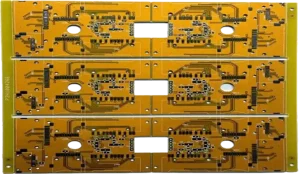
You can submit your PCB manufacturing files and specifications through the GOPCBA quotation or contact channel. The engineering team can review your requirements and provide manufacturing guidance and a quotation.
Related GOPCBA Services
- PCB Manufacturing – PCB fabrication from prototypes to volume production, including standard and advanced PCB technologies.
- PCB Design & Layout – PCB layout, stack-up design, impedance calculation, DFM, and EMC-oriented engineering support.
- PCB Assembly – SMT, THT, mixed-technology, testing, and turnkey PCB assembly.
- Prototype PCB Assembly – Prototype PCB manufacturing and assembly for early-stage product validation.
- PCB Capabilities – Detailed PCB layer, material, copper, drilling, HDI, and manufacturing capabilities.
- Components Procurement – Electronic component sourcing and inventory management for PCB assembly projects.
- Quality Management – PCB and PCBA quality control, incoming inspection, manufacturing control, and testing procedures.
- Contact GOPCBA – Submit your project requirements and request a PCB manufacturing or assembly quotation.
GOPCBA is your one-stop partner for PCB manufacturing and PCBA services, supporting PCB design, fabrication, component sourcing, assembly, testing, and production from prototype to volume manufacturing.