PCB Manufacturing
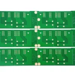
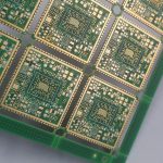
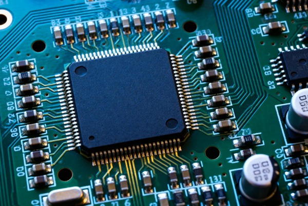
PCB manufacturing is the process of converting a PCB design into a physical, functional printed circuit board. It involves a series of controlled processes, including material preparation, circuit imaging, etching, drilling, copper plating, lamination, solder mask application, surface finishing, inspection, and electrical testing.
Modern PCB manufacturing supports a wide range of board technologies, from simple single-sided PCBs to complex multilayer, flexible, rigid-flex, HDI, high-frequency, and high-speed circuit boards.
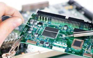
A professional PCB manufacturing process must balance electrical performance, mechanical reliability, dimensional accuracy, material selection, manufacturability, cost, and production volume.
For customers requiring both bare-board fabrication and assembly, PCB manufacturing can also be integrated with PCB assembly to provide a complete electronics manufacturing workflow.
What Is PCB Manufacturing?
PCB manufacturing, also called PCB fabrication, is the process of transforming a PCB layout into a finished bare circuit board.
A PCB typically consists of conductive copper layers separated by insulating dielectric materials. Copper traces, pads, vias, and other conductive structures provide electrical connections between components, while the substrate provides mechanical support and electrical insulation.
Depending on the application, PCBs can be classified into several major categories:
- Single-sided PCBs
- Double-sided PCBs
- Multilayer PCBs
- Rigid PCBs
- Flexible PCBs
- Rigid-flex PCBs
- HDI PCBs
- High-speed PCBs
- High-frequency and RF PCBs
- Metal-core PCBs
- Ceramic PCBs
- Heavy-copper PCBs
A typical PCB fabrication process may include material cutting, inner-layer imaging, etching, lamination, drilling, copper plating, outer-layer imaging, solder mask application, surface finishing, silkscreen printing, electrical testing, and final inspection.
For complete board fabrication and assembly requirements, see the PCB Manufacturing Service.
PCB Manufacturing Capabilities
Modern PCB manufacturers need to support different board structures, materials, layer counts, and advanced interconnection technologies.
Typical capabilities include:
PCB Types
- Rigid PCB
- Flexible PCB
- Rigid-flex PCB
- Multilayer PCB
- HDI PCB
- High-speed PCB
- High-frequency PCB
- RF and microwave PCB
- Metal-core PCB
- Ceramic PCB
- IC substrate and advanced substrate technologies
PCB Materials
Common PCB materials include:
- FR-4
- High-Tg FR-4
- Polyimide
- Kapton
- PET
- Aluminum
- Copper
- Metal-core laminates
- Ceramic
- Alumina
- PTFE
- Teflon-based high-frequency materials
- High-speed laminate materials
- Halogen-free materials
- Hybrid dielectric materials
Material selection depends on electrical requirements, operating temperature, mechanical stress, thermal management, signal frequency, impedance requirements, and application environment.
Advanced PCB Technologies
PCB manufacturing can also incorporate advanced technologies such as:
- Blind vias
- Buried vias
- Microvias
- Stacked microvias
- Staggered microvias
- Via-in-pad
- Conductive via filling
- Non-conductive via filling
- Back drilling
- Controlled impedance
- Embedded components
- Heavy copper
- Gold fingers
- High-density interconnect structures
Layer Count and Board Size
Production capability varies between manufacturers. Modern PCB fabrication can support everything from simple 1-layer boards to complex multilayer designs.
For example, advanced manufacturing platforms can support:
- 1–48 layer PCB production
- Fine-pitch trace and spacing
- Microvia structures
- High copper weights
- Controlled impedance
- Large-format PCB panels
Actual capability depends on the PCB material, stack-up, layer count, copper thickness, aspect ratio, minimum feature size, and production requirements.
Why PCB Manufacturing Quality Matters
The PCB is the physical foundation of an electronic product. Poor fabrication quality can result in electrical failures, assembly problems, premature field failures, and increased production costs.
Important PCB quality factors include:
Dimensional Accuracy
Board dimensions, hole locations, layer registration, and copper features must remain within specified tolerances.
Electrical Performance
Trace geometry, dielectric properties, copper thickness, and impedance must meet the requirements of the circuit design.
Mechanical Reliability
The board must withstand assembly processes, thermal cycling, vibration, shock, and environmental conditions appropriate to the application.
Surface Quality
Copper pads and other exposed conductive surfaces must have a suitable finish for reliable soldering, electrical contact, and long-term protection.
Interlayer Reliability
Multilayer PCBs depend on reliable connections between conductive layers. Proper lamination, drilling, desmear, and copper plating are therefore critical.
History of PCB Manufacturing
The development of PCB technology has closely followed the evolution of modern electronics.
1903 – Early Printed Wiring Concepts
Albert Hanson, a German inventor, patented an early printed-wire concept involving conductive paths on an insulating substrate. His work represented an important early step toward modern printed circuit technology.
1936 – Early Practical PCB Development
Austrian inventor Paul Eisler developed a radio using conductive copper patterns on an insulating substrate. His work helped establish the concept of using printed circuitry in electronic products.
1940s – Expansion of Electronic Manufacturing
The development of modern electronics during and after World War II accelerated the need for more efficient electrical interconnection methods. PCB technology became increasingly important for electronic equipment.
1950s and 1960s – Multilayer PCB Development
The rapid development of aerospace, defense, communications, and computing technologies encouraged advances in multilayer PCB structures and more sophisticated interconnection methods.
1970s – Microelectronics
The increasing use of integrated circuits and microprocessors created demand for PCBs capable of supporting higher component density and more complex electrical connections.
1990s – Mobile and Internet Electronics
The expansion of personal computers, mobile phones, and internet infrastructure accelerated PCB miniaturization and manufacturing technology.
2000s to Today – High-Density Electronics
Smartphones, IoT devices, automotive electronics, medical equipment, artificial intelligence, and high-speed computing have continued to drive PCB manufacturing toward smaller geometries, higher layer counts, advanced materials, and higher signal integrity.
Common Types of PCBs
PCB classification is generally based on the number of conductive layers, substrate material, construction, and intended application.
Single-Sided PCB
A single-sided PCB has one conductive copper layer on one side of the insulating substrate.
Because of its simple construction, it is generally economical to manufacture and is suitable for applications with relatively low circuit complexity.
Typical applications include:
- Consumer electronics
- Power supplies
- Basic control circuits
- LED products
- Simple industrial electronics
Double-Sided PCB
A double-sided PCB has copper layers on both sides of the substrate.
Plated through-holes and vias provide electrical connections between the top and bottom copper layers. Compared with single-sided boards, double-sided PCBs provide greater routing flexibility and support higher circuit density.
Multilayer PCB
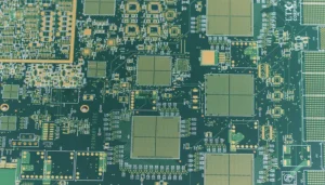
A multilayer PCB contains three or more conductive copper layers separated by dielectric materials.
Internal layers can be used for:
- Signal routing
- Ground planes
- Power distribution
- High-speed signal transmission
- Electromagnetic shielding
Multilayer construction allows designers to achieve greater circuit density while maintaining controlled electrical performance.
Multilayer PCBs are widely used in computers, telecommunications equipment, industrial electronics, medical devices, automotive electronics, networking equipment, and aerospace systems.
Rigid PCB
Rigid PCBs are manufactured from non-flexible substrates such as FR-4, metal-core laminates, ceramic, or other rigid materials.
They provide mechanical support for electronic components and are the most common PCB construction used across general electronics.
Flexible PCB
Flexible PCBs use bendable substrates, commonly polyimide, to enable electrical connections in compact or moving applications.
Key advantages include:
- Reduced weight
- Reduced package size
- Improved space utilization
- Ability to bend and fold
- Fewer connectors and cables
- Suitable for dynamic applications
Flexible PCBs are commonly used in cameras, mobile devices, wearable electronics, medical equipment, automotive systems, and compact consumer products.
Rigid-Flex PCB
Rigid-flex PCBs combine rigid circuit sections with flexible circuit sections in a single integrated structure.
The rigid sections provide mechanical support and component mounting areas, while flexible sections provide electrical connections between different rigid sections.
This construction can reduce connectors, cables, assembly complexity, and overall product size.
Rigid-flex PCBs are commonly used in:
- Aerospace electronics
- Medical equipment
- Automotive systems
- Cameras
- Portable electronics
- Robotics
- Advanced industrial equipment
PCB Materials
Material selection has a direct impact on PCB electrical, thermal, mechanical, and reliability performance.
Dielectric Substrate
The dielectric material provides electrical insulation between conductive layers.
FR-4 is one of the most widely used PCB materials. It is based on glass fiber reinforcement combined with epoxy resin.
Other dielectric materials may be selected when applications require higher thermal resistance, lower dielectric loss, controlled electrical characteristics, flexibility, or high-frequency performance.
Core Material
A PCB core is a rigid dielectric structure with copper foil laminated to one or both sides.
Core materials form the fundamental building blocks of multilayer PCB stack-ups.
Prepreg
Prepreg is a resin-impregnated glass-fiber material used to bond PCB layers together during multilayer lamination.
During the lamination process, heat and pressure cause the resin to flow and cure, creating a solid multilayer structure.
Prepreg selection affects:
- Layer thickness
- Dielectric thickness
- Impedance
- Lamination reliability
- Thermal performance
- Electrical characteristics
Copper Foil
Copper provides the conductive paths used for traces, pads, planes, and other electrical structures.
Copper thickness is commonly specified by weight or thickness. Standard applications may use relatively light copper, while power electronics and high-current applications may require heavy copper.
Solder Mask
Solder mask is a protective polymer layer applied over the PCB surface.
It helps:
- Protect exposed copper
- Reduce oxidation
- Prevent solder bridges
- Improve electrical insulation
- Define solderable areas
Silkscreen
Silkscreen is used to print identification information on the PCB, including:
- Component references
- Polarity markings
- Logos
- Test points
- Assembly instructions
- Product identification
Vias in PCB Manufacturing
Vias are conductive structures used to electrically connect different PCB layers.
Through Vias
Through vias extend through the entire PCB and connect multiple conductive layers.
They are widely used because they are relatively simple and cost-effective to manufacture.
Blind Vias
Blind vias connect an external layer to one or more internal layers without passing through the entire PCB.
They help increase routing density and are commonly used in HDI designs.
Buried Vias
Buried vias connect internal layers without reaching the outer surfaces of the PCB.
They allow designers to use internal space more efficiently.
Microvias
Microvias are very small vias, typically produced using laser drilling.
They are widely used in HDI PCBs and support fine-pitch components and high-density routing.
Because via fabrication involves drilling, desmear, plating, and sometimes filling processes, via structures can significantly affect PCB manufacturing cost and reliability.
PCB Manufacturing Process
PCB fabrication consists of multiple controlled production stages. The exact process varies according to board structure, materials, layer count, technology, and performance requirements.
1. Engineering Review and DFM
PCB manufacturing begins with an engineering review of the customer’s design files.
Typical inputs include:
- Gerber files
- Drill files
- Stack-up information
- Fabrication drawings
- Netlist
- Impedance requirements
- Material specifications
- Surface finish requirements
During DFM analysis, engineers review trace width, spacing, hole sizes, annular rings, copper distribution, layer registration, solder mask, panelization, and other manufacturing factors.
The goal is to identify potential production risks before fabrication begins.
2. Material Preparation and Cutting
The selected laminate, copper foil, prepreg, and other materials are prepared according to the specified board stack-up.
Large sheets are cut into production panels suitable for subsequent fabrication processes.
3. Inner-Layer Imaging
For multilayer PCBs, circuit patterns are transferred onto the copper surface of the inner-layer cores.
Photolithography or laser direct imaging technology can be used to create highly accurate circuit patterns.
4. Etching
Unwanted copper is chemically removed from the panel, leaving the required traces, pads, planes, and other conductive structures.
After etching, the remaining circuit pattern is inspected to verify dimensional accuracy and potential defects.
5. Layer Registration and Lamination
For multilayer PCBs, inner-layer cores and prepreg materials are carefully stacked according to the designed layer structure.
Heat and pressure are applied during lamination to bond the layers into a solid PCB structure.
Precise layer alignment is essential because registration errors can affect vias, traces, pads, and overall electrical performance.
6. Drilling
Mechanical or laser drilling creates holes for component leads and interlayer electrical connections.
Depending on the design, drilling may include:
- Mechanical through-holes
- Blind vias
- Buried vias
- Laser microvias
- Back-drilled holes
Drilling quality is influenced by tool condition, material properties, hole diameter, aspect ratio, and drilling parameters.
7. Desmear and Copper Plating
After drilling, resin residues may remain inside the holes. Desmear processes remove unwanted material and prepare the hole walls for plating.
A conductive seed layer is then created, followed by copper plating.
Copper plating forms a reliable conductive connection between PCB layers through plated holes and vias.
8. Outer-Layer Imaging and Etching
The outer copper layers are patterned according to the PCB design.
Unwanted copper is removed through controlled etching, leaving the required traces, pads, planes, and other conductive features.
9. Solder Mask Application
A solder mask layer is applied to protect the copper surface and define areas that need to remain exposed for soldering or electrical contact.
The solder mask is exposed, developed, and cured according to the selected manufacturing process.
10. Surface Finish
Exposed copper pads require an appropriate surface finish to protect them from oxidation and provide reliable solderability.
Common PCB surface finishes include:
- HASL
- Lead-free HASL
- OSP
- ENIG
- ENEPIG
- Immersion silver
- Immersion tin
- Hard gold
- Selective surface finishes
HASL
Hot Air Solder Leveling coats exposed copper with solder and uses hot air to remove excess solder.
HASL is a cost-effective option for many conventional PCB applications.
OSP
Organic Solderability Preservative uses a thin organic coating to protect exposed copper while maintaining solderability.
OSP is commonly selected when a flat surface is important.
ENIG
Electroless Nickel Immersion Gold deposits a nickel layer followed by a thin immersion gold layer.
ENIG provides a flat surface and good solderability, making it popular for fine-pitch and advanced PCB applications.
ENEPIG
ENEPIG adds a palladium layer between nickel and gold.
It can be selected for applications requiring high reliability, wire bonding, and demanding surface performance.
11. Silkscreen Printing
Identification markings and assembly information are printed onto the PCB surface.
The information may include reference designators, polarity indicators, labels, logos, and other manufacturing information.
12. Electrical Testing
Electrical testing verifies the connectivity of the finished PCB.
Depending on production volume and board complexity, manufacturers may use flying probe testing, fixture-based testing, or other automated electrical test methods.
13. Final Inspection
Finished PCBs undergo final inspection to verify:
- Board dimensions
- Surface condition
- Copper features
- Solder mask
- Silkscreen
- Hole quality
- Surface finish
- Warpage
- Electrical performance
Only boards meeting the specified requirements should proceed to packaging and shipment.
Multilayer PCB Manufacturing
Multilayer PCB fabrication requires additional processes compared with single- and double-sided boards.
A typical multilayer structure includes:
- Copper foil
- Prepreg
- Inner-layer cores
- Prepreg
- Copper foil
The exact stack-up depends on the required layer count, impedance, dielectric thickness, copper weight, signal integrity, and mechanical requirements.
The major steps include:
- Inner-layer circuit formation
- Inner-layer inspection
- Layer stacking
- Lamination
- Drilling
- Desmear
- Copper plating
- Outer-layer imaging
- Etching
- Solder mask
- Surface finishing
- Silkscreen
- Electrical testing
- Final inspection
For high-density applications, multilayer boards may also incorporate blind vias, buried vias, microvias, via filling, sequential lamination, and controlled impedance structures.
HDI PCB Manufacturing
High-Density Interconnect, or HDI, technology enables higher circuit density within a smaller PCB footprint.
HDI manufacturing may incorporate:
- Laser microvias
- Blind vias
- Buried vias
- Stacked microvias
- Staggered microvias
- Via-in-pad
- Sequential lamination
- Fine-line circuitry
- High-density component routing
HDI PCBs are widely used in smartphones, portable electronics, medical equipment, automotive electronics, networking devices, wearable products, and other miniaturized electronic systems.
The manufacturing process requires tighter control of registration, laser drilling, dielectric thickness, copper plating, and microvia reliability.
PCB Testing and Inspection
PCB quality control includes both visual inspection and electrical testing.
Manufacturing defects can generally be divided into cosmetic defects and functional defects.
Cosmetic and Manufacturing Defects
Examples include:
- Scratches
- Pinholes
- Excessive etching
- Under-etching
- Solder mask defects
- Silkscreen defects
- Copper exposure
- Board warpage
Functional Defects
Functional problems can include:
- Open circuits
- Short circuits
- Incorrect connections
- Poor plated-through-hole connections
- Insufficient copper thickness
- Interlayer connectivity failures
Testing and inspection help identify these problems before the PCB reaches the assembly stage.
Automated Optical Inspection
Automated Optical Inspection, commonly called AOI, uses cameras and image-processing systems to inspect PCB features.
AOI systems can identify potential problems such as:
- Missing or damaged features
- Incorrect trace geometry
- Short circuits
- Open circuits
- Solder mask registration issues
- Surface defects
AOI provides fast and repeatable inspection for modern PCB production.
In-Circuit Testing
In-Circuit Testing, or ICT, uses electrical test fixtures and probes to verify circuit connectivity and component-related characteristics.
ICT is particularly useful for production environments where repeatable testing of large quantities of boards is required.
It can help identify:
- Open circuits
- Short circuits
- Resistance problems
- Capacitance problems
- Incorrect connections
Flying Probe Testing
Flying probe testing uses programmable probes that move across designated test points on the PCB.
Unlike traditional fixture-based ICT, flying probe systems generally do not require a dedicated test fixture.
This makes flying probe testing particularly suitable for:
- Prototypes
- Engineering samples
- Low-volume production
- Frequently changing designs
- Complex boards
PCB Manufacturing Applications
PCB manufacturing supports virtually every major electronics industry.
Consumer Electronics
Consumer electronics represent one of the largest PCB application markets.
Typical products include:
- Smartphones
- Tablets
- Laptops
- Smart home devices
- Wearable electronics
- Cameras
- Entertainment systems
The trend toward smaller and more feature-rich devices continues to increase demand for flexible, rigid-flex, HDI, and high-density multilayer PCBs.
Industrial Automation and Control
Industrial automation systems require reliable PCBs for control, communication, sensing, and power management.
Applications include:
- PLC systems
- Robotics
- Motion controllers
- Industrial computers
- Motor control
- Sensors
- Measurement equipment
- Factory automation systems
Depending on the application, industrial electronics may require rigid, flexible, multilayer, high-Tg, or other specialized PCB technologies.
Power Electronics and Energy
Power electronics require PCBs capable of handling high current, elevated temperatures, and demanding electrical conditions.
Applications include:
- Power supplies
- UPS systems
- Battery management systems
- Solar energy equipment
- Energy storage systems
- Electric vehicle electronics
- Power converters
- Motor controllers
Heavy-copper PCB technology and high-Tg materials may be selected for demanding thermal and current-carrying requirements.
Automotive Electronics
Automotive electronics require high reliability and consistent manufacturing quality because PCBs are exposed to temperature changes, vibration, humidity, and other environmental stresses.
PCB applications include:
- ADAS
- Automotive cameras
- Infotainment
- Battery management systems
- Vehicle control units
- Sensors
- Lighting systems
- Power electronics
- Safety systems
As electric vehicles and advanced driver assistance systems continue to develop, PCB requirements are becoming increasingly sophisticated.
Medical Electronics
Medical electronics require reliable and precisely manufactured circuit boards.
PCB applications include:
- Patient monitoring equipment
- Diagnostic instruments
- Portable medical devices
- Imaging equipment
- Laboratory equipment
- Medical control systems
- Implantable and wearable electronics
Depending on the application, medical PCBs may require strict process control, traceability, specialized materials, and rigorous testing.
Telecommunications and Networking
Communication equipment often requires high-speed and high-frequency PCB technologies.
Typical applications include:
- Network equipment
- Wireless communication systems
- RF equipment
- Data transmission systems
- Routers
- Switches
- Base stations
- High-speed computing equipment
Signal integrity, controlled impedance, low dielectric loss, and thermal management are important considerations in these applications.
Aerospace and Defense
Aerospace and defense electronics demand high reliability under demanding operating conditions.
PCB requirements may include:
- High-temperature materials
- Low-loss materials
- High-reliability multilayer construction
- Controlled impedance
- High-density interconnects
- Advanced inspection and testing
- Strong process traceability
PCB Manufacturing Quality Standards
Quality management is a critical part of PCB fabrication.
Manufacturers may work according to internationally recognized standards and customer-specific specifications.
Important industry standards include:
- IPC-A-600
- IPC-A-6012
- IPC-A-6013
- IPC-2221
- IPC-4101
- ISO 9001
- ISO 13485
- IATF 16949
- UL requirements
- RoHS requirements
The appropriate standard depends on the PCB type, industry, product application, and customer requirements.
Quality control should cover incoming materials, production processes, dimensional inspection, electrical testing, final inspection, and traceability.
How to Choose a PCB Manufacturing Partner
Choosing the right PCB manufacturer can significantly affect product quality, development speed, and overall manufacturing cost.
Consider the following factors:
Manufacturing Capability
Confirm that the manufacturer can support the required layer count, materials, copper thickness, minimum trace and spacing, hole sizes, impedance requirements, and PCB technology.
Engineering Support
Experienced engineers can identify DFM issues before production and recommend manufacturing improvements.
Quality Control
Review the manufacturer’s inspection, electrical testing, material control, process monitoring, and traceability procedures.
Production Capacity
Make sure the manufacturer can support your expected prototype, low-volume, and mass-production requirements.
Lead Time
Production schedules depend on board complexity, materials, layer count, technology, and quantity. A capable supplier should provide realistic lead-time estimates rather than relying only on standard delivery promises.
Communication
Responsive engineering and customer service teams can help reduce delays when technical questions, design changes, or production issues arise.
Integrated Manufacturing
A supplier capable of providing both PCB fabrication and PCB assembly can simplify the supply chain and reduce coordination between multiple vendors.
For integrated manufacturing requirements, see the PCB Assembly Service.
PCB Manufacturing and PCB Assembly
PCB fabrication produces the bare circuit board, while PCB assembly installs electronic components onto the fabricated PCB.
A complete electronics manufacturing workflow may include:
- PCB design
- DFM review
- PCB fabrication
- Component sourcing
- Solder paste printing
- SMT placement
- Reflow soldering
- Through-hole assembly
- AOI inspection
- X-ray inspection
- Functional testing
- Final assembly
- Packaging and shipment
Combining PCB manufacturing and PCB assembly under one supply chain can simplify project management and reduce logistics between different suppliers.
For detailed manufacturing capability information, visit the PCB Capabilities page.
PCB Manufacturing Trends
PCB technology continues to evolve as electronic products become smaller, faster, more connected, and more intelligent.
Miniaturization
Smaller electronic devices require higher circuit density and smaller interconnection structures.
HDI, microvias, fine-line technology, and rigid-flex construction are increasingly important for compact products.
High-Speed Electronics
The growth of high-speed computing, telecommunications, artificial intelligence, and networking equipment is increasing demand for low-loss materials and controlled-impedance PCB structures.
Electric Vehicles
Electric vehicles require large numbers of electronic control systems, sensors, power electronics, battery management systems, and communication modules.
This creates demand for high-reliability and thermally capable PCB technologies.
IoT
Internet of Things devices require compact, energy-efficient, and reliable electronics.
Flexible and rigid-flex PCBs can help manufacturers integrate electronics into space-constrained products.
Artificial Intelligence
AI hardware is driving demand for high-speed interconnects, advanced packaging, higher-density PCBs, and improved thermal management.
Advanced HDI
Sequential lamination, stacked microvias, via-in-pad technology, and fine-line structures are enabling increasingly sophisticated PCB designs.
Sustainable Manufacturing
Environmental considerations are becoming more important throughout the PCB supply chain.
Manufacturers are increasingly focusing on:
- Halogen-free materials
- Lead-free processes
- Chemical management
- Energy efficiency
- Waste reduction
- Material recycling
- More efficient manufacturing processes
Frequently Asked Questions About PCB Manufacturing
What is PCB manufacturing?
PCB manufacturing is the process of producing a physical printed circuit board from an electronic design. It includes material preparation, circuit imaging, etching, drilling, lamination, copper plating, solder mask, surface finishing, testing, and inspection.
What is the difference between PCB manufacturing and PCB assembly?
PCB manufacturing produces the bare circuit board. PCB assembly installs electronic components onto the fabricated board using processes such as SMT, through-hole assembly, soldering, inspection, and testing.
What materials are commonly used for PCB manufacturing?
FR-4 is the most common general-purpose PCB material. Other materials include high-Tg laminates, polyimide, PTFE, ceramic, aluminum, copper, high-speed laminates, and other specialized dielectric materials.
What is an HDI PCB?
An HDI PCB is a high-density interconnect circuit board that uses technologies such as microvias, blind vias, buried vias, fine-line circuitry, and sequential lamination to achieve higher routing density.
What surface finish is best for a PCB?
There is no single surface finish that is best for every application. HASL, lead-free HASL, OSP, ENIG, ENEPIG, immersion silver, immersion tin, and hard gold each offer different combinations of cost, flatness, solderability, durability, and application suitability.
How long does PCB manufacturing take?
Lead time depends on board complexity, material availability, layer count, copper thickness, technology, quantity, testing requirements, and shipping method. Prototype boards can often be manufactured much faster than complex high-volume production orders.
What files are required for PCB manufacturing?
Typical manufacturing data includes Gerber files, drill files, fabrication drawings, stack-up information, material specifications, surface finish requirements, impedance requirements, and other production documentation.
Get a PCB Manufacturing Quote
A reliable PCB manufacturing partner should provide more than basic fabrication. Engineering support, material selection, DFM analysis, process control, testing, quality assurance, and responsive communication all contribute to successful PCB production.
Whether you need a simple single-sided PCB, a multilayer board, flexible PCB, rigid-flex PCB, HDI PCB, high-frequency PCB, or high-speed circuit board, selecting a manufacturer with the right technical capabilities is essential.
For complete project support, you can also review the PCBA Capabilities available for PCB assembly and electronics manufacturing.
To discuss your PCB requirements, submit your Gerber files, specifications, quantity, and target delivery schedule through the Contact Us page.
A professional PCB manufacturing workflow can help reduce production risks, improve product reliability, shorten development cycles, and provide a scalable path from prototype to volume production.