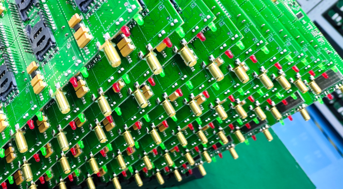
PCB fabrication is the manufacturing process that transforms digital PCB design files into finished bare printed circuit boards. It combines precision imaging, etching, lamination, drilling, copper plating, solder mask application, surface finishing, inspection, and electrical testing to produce reliable circuit boards for applications ranging from consumer electronics and industrial automation to automotive, medical, aerospace, telecommunications, AI infrastructure, and power electronics.
As electronic products become smaller, faster, and more complex, the PCB fabrication process must deliver increasingly fine circuit features, tighter layer registration, improved signal integrity, better thermal management, and higher manufacturing consistency.
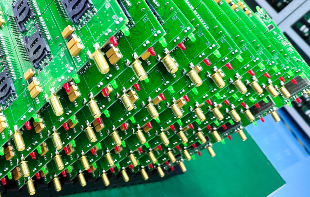
Although the exact process varies according to board structure and application requirements, most multilayer PCB manufacturing follows a structured sequence:
Engineering Review → Inner-Layer Fabrication → Lamination → Drilling → Copper Plating → Outer-Layer Imaging → Etching → Solder Mask → Surface Finish → Electrical Testing → Final Inspection → Packaging
Understanding the complete PCB manufacturing process helps engineers make better design decisions, improve manufacturability, reduce manufacturing risks, increase production yield, and achieve a smoother transition from prototype to mass production.
PCB Fabrication Process at a Glance
A modern PCB fabrication process is a highly controlled manufacturing workflow designed to convert electronic design data into a reliable bare PCB ready for assembly.
The major stages include:
1. Front-End Engineering
Manufacturing files are reviewed, DFM checks are performed, stackup requirements are verified, and production tooling data is prepared.
2. Inner-Layer Fabrication
Copper-clad laminate cores are cleaned, photoresist is applied, circuit patterns are imaged, unwanted copper is etched away, and inner layers are inspected.
3. Layer Stack-Up and Lamination
Inner-layer cores, prepreg, and copper foil are precisely aligned and bonded using controlled heat and pressure to create a multilayer PCB.
4. Drilling
Mechanical drilling and laser drilling create through-holes, blind vias, buried vias, and microvias according to the PCB design.
5. Hole Preparation and Copper Deposition
Drilled holes are deburred and desmeared before electroless copper deposition creates a conductive seed layer.
6. Outer-Layer Imaging and Pattern Plating
Outer-layer circuit patterns are formed, copper is plated to the required thickness, and unwanted copper is etched away.
7. Solder Mask, Silkscreen, and Surface Finish
Protective solder mask is applied, component markings are printed, and a suitable surface finish is applied to exposed copper pads.
8. Electrical Testing and Inspection
Finished boards undergo electrical testing, AOI, dimensional inspection, and visual inspection to verify compliance with design requirements.
9. Packaging and Shipment
Finished PCBs are packaged using appropriate ESD and moisture protection before shipment to the customer or PCB assembly facility.
Typical PCB Fabrication Lead Times
Lead times depend on layer count, PCB dimensions, materials, technology, order quantity, testing requirements, and production capacity.
| PCB Type | Typical Lead Time |
|---|---|
| Standard 2–4 Layer PCB | 3–7 business days |
| Quick-Turn Prototype PCB | 1–3 business days |
| Multilayer PCB | 5–15 business days |
| HDI PCB | 1–3 weeks |
| Rigid-Flex PCB | 2–4 weeks |
| Advanced High-Frequency PCB | Typically longer, depending on materials and construction |
These are general industry ranges rather than guaranteed delivery times. Actual production schedules should be confirmed after engineering review.
1. PCB Manufacturing Begins with Front-End Engineering
A PCB does not begin as a physical product. It starts with a digital manufacturing package containing the data required to fabricate the circuit board.
Typical files include:
- Gerber files
- ODB++ or IPC-2581 data
- NC drill files
- Routing files
- PCB stackup information
- Fabrication drawings
- Material specifications
- Copper requirements
- Surface-finish requirements
- Controlled-impedance specifications
Before production begins, manufacturing engineers review these files to ensure that the proposed construction is manufacturable.
DFM Analysis
Design for Manufacturability (DFM) is one of the most important steps in the PCB manufacturing process.
Engineers review:
- Minimum trace width
- Minimum spacing
- Hole diameter
- Annular ring
- Copper-to-edge clearance
- Solder-mask clearance
- Layer registration
- Aspect ratio
- Impedance requirements
- Via structures
- Material compatibility
The manufacturing team may also review the design netlist to identify potential connectivity discrepancies.
Early DFM review can prevent problems from reaching production, reducing redesigns, delays, and material waste.
PCB Panelization
PCBs are usually manufactured in panels rather than individually.
Multiple boards are arranged onto a larger production panel to improve:
- Material utilization
- Machine efficiency
- Production throughput
- Handling efficiency
- Assembly compatibility
An optimized panel layout is particularly important for PCB prototype manufacturing and high-volume PCB production, where material utilization directly affects manufacturing economics.
CAM Engineering
CAM engineers convert design data into production-ready manufacturing files.
These may include:
- LDI data
- CNC drilling programs
- Routing programs
- Solder-mask artwork
- Silkscreen artwork
- Electrical-test data
- Tooling-hole information
- Fiducial locations
- Test coupons
The goal is to ensure that the digital design can be translated accurately into a physical board.
2. How Inner PCB Layers Are Manufactured
For a multilayer PCB, internal copper layers are manufactured before the layers are laminated together.
These internal layers may contain:
- Signal routing
- Ground planes
- Power planes
- High-speed transmission lines
Surface Preparation
Copper-clad laminate is carefully cleaned to remove:
- Oxidation
- Oil
- Dust
- Fingerprints
- Other surface contaminants
A clean copper surface is essential for reliable photoresist adhesion and accurate circuit imaging.
Photoresist Lamination
A photosensitive dry-film photoresist is laminated onto the copper surface.
The photoresist acts as a temporary protective layer during imaging and etching.
Laser Direct Imaging
Modern PCB manufacturers increasingly use Laser Direct Imaging (LDI) to transfer the circuit pattern onto the photoresist.
LDI provides several advantages:
- High imaging accuracy
- Better layer-to-layer registration
- Reduced phototool distortion
- Support for fine-line PCB fabrication
- Improved consistency for HDI and high-density designs
This technology is particularly valuable for HDI PCB manufacturing and advanced multilayer boards.
Develop, Etch, and Strip
After imaging, the panel passes through a Develop-Etch-Strip process.
The basic sequence is:
Develop → Etch → Strip
Unwanted photoresist is removed, exposed copper is etched away, and the remaining photoresist is stripped from the panel.
The result is the desired internal copper circuit pattern.
Inner-Layer AOI
Each completed inner layer is inspected before lamination.
AOI (Automated Optical Inspection) compares the actual copper pattern with the manufacturing data to detect:
- Shorts
- Opens
- Missing copper
- Excess copper
- Under-etching
- Over-etching
- Pattern defects
Identifying defects before lamination is critical because an internal-layer defect becomes difficult and expensive to correct once the multilayer structure is completed.
3. How PCB Layers Are Laminated Together
Once all inner layers pass inspection, they are stacked and laminated into a multilayer structure.
A typical stackup may include:
Copper Foil + Prepreg + Inner-Layer Core + Prepreg + Copper Foil
The exact construction depends on the required layer count, electrical performance, thickness, impedance, and application.
Copper Surface Treatment
Before lamination, inner copper surfaces receive oxide or oxide-alternative treatment.
This improves the bonding characteristics between the copper and prepreg resin.
Layer Stack-Up
Manufacturing technicians follow the approved PCB stackup and carefully position:
- Inner-layer cores
- Prepreg
- Copper foil
- Separation materials
- Tooling components
Advanced optical registration systems and tooling pins help maintain accurate layer alignment.
Lamination Pressing
The stacked panels are placed into a lamination press.
Controlled combinations of:
- Temperature
- Pressure
- Vacuum
- Time
are used to cure the prepreg resin and permanently bond all layers together.
The resin flows into microscopic gaps and bonds the structure into a rigid multilayer PCB.
Why Lamination Matters
Poor lamination can cause:
- Delamination
- Voids
- Blistering
- Layer misregistration
- Resin starvation
- Dimensional instability
Therefore, lamination is one of the most critical stages of the multilayer PCB fabrication process.
4. PCB Drilling: Creating Holes and Vias
After lamination, drilling creates the holes required for electrical and mechanical connections.
Depending on PCB design, these may include:
- Through-holes
- Blind vias
- Buried vias
- Microvias
- Component holes
- Mounting holes
Mechanical Drilling
High-speed CNC drilling machines use precision carbide drill bits to create conventional through-holes and larger via structures.
Mechanical drilling is commonly used for:
- Through-hole components
- Mounting holes
- Plated through-holes
- Mechanical features
Internal-layer registration is critical because the copper circuitry is buried inside the board after lamination.
Laser Drilling
Laser drilling is particularly important for HDI PCBs.
Laser-drilled microvias enable connections between specific layers without requiring conventional through-holes that occupy routing space across the entire PCB stack.
Laser drilling supports:
- Smaller vias
- Higher wiring density
- Fine-pitch BGA breakout
- More compact PCB designs
- Sequential buildup structures
Kingda’s published PCB capabilities support HDI manufacturing with laser-drilled microvias, stacked microvias, copper-filled microvias, and buried filled vias. Its listed minimum laser-drill capability is down to 0.08 mm in advanced fabrication. (Kingda)
5. Hole Preparation and Copper Plating
Drilling alone does not make the holes electrically conductive.
The drilled holes must be cleaned and copper-plated to establish reliable electrical connections between layers.
Deburring
Mechanical drilling may leave:
- Burrs
- Copper debris
- Resin residue
These contaminants are removed before plating.
Desmear
During drilling, heat and mechanical friction can cause epoxy resin to smear over internal copper pads.
A chemical or plasma desmear process removes this resin and exposes the underlying copper.
Proper desmear is essential for reliable electrical contact.
Electroless Copper
The panels then undergo electroless copper deposition.
This chemical process deposits a thin conductive copper layer over:
- Hole walls
- Copper surfaces
- Fiberglass
- Resin surfaces
The electroless copper creates the conductive foundation needed for subsequent electrolytic copper plating.
Electrolytic Copper Plating
The next stage increases copper thickness on:
- Hole walls
- Vias
- Outer-layer copper
Controlled plating parameters help achieve consistent copper thickness and reliable plated-through-hole performance.
6. Outer-Layer PCB Imaging, Plating, and Etching
After drilling and hole plating, the outer circuit layers are formed.
Outer-Layer Imaging
A photosensitive photoresist is applied to the outer copper surfaces.
The circuit pattern is transferred using LDI or another imaging method.
Pattern Plating
Copper is electroplated onto the exposed circuit areas.
This simultaneously builds the copper thickness of traces, pads, and plated holes.
Tin Plating
Tin can be applied as an etch-resistant protective layer over the finished copper pattern.
Final Etching
The unwanted copper is chemically removed while the desired circuit features remain protected.
After the temporary protective layer is removed, the finished external copper circuitry becomes visible.
This stage determines the final geometry of:
- Signal traces
- Pads
- Ground planes
- Power planes
- Plated holes
Precise control of etching is especially important for fine-line PCB manufacturing and high-speed circuit boards.
7. Solder Mask, Silkscreen, and Surface Finish
After circuit fabrication is complete, the PCB enters the finishing stage.
Solder Mask
Solder mask is a protective polymer coating that covers most of the exposed copper.
Its functions include:
- Preventing solder bridges
- Protecting copper from oxidation
- Improving electrical insulation
- Increasing environmental resistance
- Protecting against mechanical damage
Modern PCB manufacturing commonly uses Liquid Photoimageable (LPI) solder mask.
Silkscreen
Silkscreen, or PCB legend, provides information such as:
- Component reference designators
- Polarity indicators
- Pin-1 markers
- Logos
- Revision information
- Assembly instructions
This information is particularly useful during PCB assembly, inspection, maintenance, and repair.
PCB Surface Finish
A surface finish protects exposed copper pads and maintains solderability.
Common options include:
ENIG
Electroless Nickel Immersion Gold provides a flat surface and is widely used for fine-pitch SMT and BGA applications.
HASL
Hot Air Solder Leveling is a cost-effective option for many general-purpose PCB applications.
Immersion Silver
Provides a flat surface suitable for fine-pitch components and selected high-performance applications.
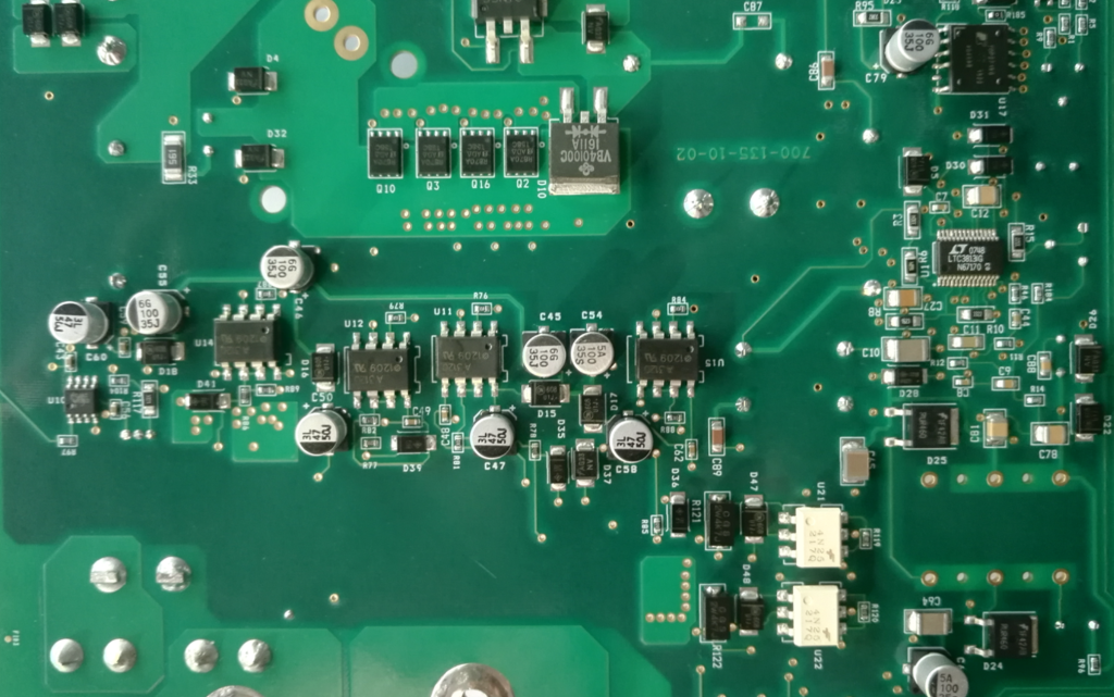
ENEPIG
Electroless Nickel Electroless Palladium Immersion Gold is commonly selected for demanding applications requiring excellent solderability and surface reliability.
Kingda’s PCB manufacturing capabilities cover a broad range of PCB structures and technologies, including high-frequency PCB, high-TG PCB, thick-copper PCB, HDI PCB, impedance-controlled PCB, metal-base PCB, rigid-flex PCB, and advanced multilayer PCB manufacturing. (Kingda)
8. PCB Electrical Testing and Inspection
Before shipment, the finished PCB undergoes multiple quality checks.
Electrical Testing
Electrical tests verify that the PCB matches its intended circuit connectivity.
Typical tests detect:
- Opens
- Shorts
- Incorrect connections
- Isolation failures
Flying Probe Testing
Flying probe systems are suitable for:
- Prototype PCBs
- Low-volume production
- Frequently changing designs
They reduce the need for dedicated test fixtures.
Bed-of-Nails Testing
Bed-of-nails testing uses a dedicated fixture to contact multiple test points simultaneously.
It is particularly suitable for high-volume PCB production where testing speed is important.
Impedance Testing
For high-speed PCB and RF designs, impedance testing verifies that controlled-impedance traces meet specified electrical characteristics.
Test coupons are commonly fabricated alongside production panels for impedance verification.
Dimensional Inspection
The manufacturer may verify:
- Length
- Width
- Thickness
- Hole size
- Hole position
- Layer registration
- Board-edge dimensions
Final Visual Inspection
Final inspection evaluates:
- Solder-mask registration
- Surface finish
- Silkscreen
- Copper defects
- Board edges
- Mechanical features
- Overall workmanship
9. PCB Depanelization, Packaging, and Shipment
Once electrical and quality testing is complete, the PCB panels are separated into individual boards.
Common depanelization methods include:
- CNC routing
- V-scoring
- Tab routing
- Laser cutting for specialized applications
After depanelization, boards are packaged to protect them against:
- Moisture
- Electrostatic discharge
- Mechanical damage
- Oxidation
For sensitive PCB products, ESD-safe moisture-barrier packaging with desiccants and humidity indicators can be used.
Factors That Affect PCB Fabrication Cost
The cost of PCB fabrication depends on much more than board size.
Important cost drivers include:
Layer Count
Higher layer counts increase:
- Material usage
- Lamination cycles
- Processing time
- Registration requirements
Material Selection
Standard FR-4 is economical for many applications, while advanced materials may be necessary for:
- High-frequency circuits
- High-speed designs
- High-temperature applications
- RF/microwave systems
- High-power electronics
Copper Thickness
Heavy-copper PCBs require additional plating and process control.
PCB Size
Larger boards consume more panel area and may reduce panel utilization.
Line Width and Spacing
Fine-line structures require more advanced imaging and etching capabilities.
Via Technology
Blind vias, buried vias, microvias, stacked microvias, and copper-filled vias increase processing requirements.
Surface Finish
ENIG and ENEPIG generally cost more than standard HASL.
Testing Requirements
Advanced electrical, impedance, microsection, reliability, and dimensional testing can also affect the total cost.
PCB Fabrication for Prototype vs. Mass Production
PCB Prototype Manufacturing
PCB prototype manufacturing emphasizes:
- Fast turnaround
- Engineering flexibility
- Rapid design iteration
- Small quantities
- DFM feedback
- Design validation
The objective is to discover potential electrical and manufacturing problems before large-scale production.
Mass PCB Production
Mass production focuses on:
- High throughput
- Repeatability
- Automated process control
- Stable component and material supply
- Cost optimization
- High production yield
A good manufacturing partner should be able to support the project from prototype PCB fabrication to volume PCB production without forcing the customer to restart the qualification process with another supplier.
Why Choose Kingda for PCB Fabrication?
Kingda provides an integrated PCB manufacturing and PCBA service, combining PCB fabrication, component procurement, PCB assembly, testing, and final product integration under one manufacturing system. Founded in 2013, the company reports more than 10 years of experience in PCB and PCBA manufacturing. (Kingda)
Broad PCB Manufacturing Capabilities
Kingda’s published fabrication capabilities cover:
- 1–48 layer PCB products
- Multilayer PCBs
- HDI PCBs
- High-TG PCBs
- Thick-copper PCBs
- High-frequency PCBs
- Rogers mixed-lamination PCBs
- Blind and buried via PCBs
- Metal-base PCBs
- Half-hole PCBs
- Gold-finger PCBs
- Impedance-controlled PCBs
- Countersunk-hole PCBs
- High-frequency antenna PCBs (Kingda)
Its published advanced fabrication specifications include up to 100 layers, a maximum panel size of 610 × 1067 mm, minimum laser-drill size of 0.08 mm, and advanced HDI structures such as stacked and copper-filled microvias. (Kingda)
Engineering and DFM Support
Kingda integrates engineering support into its manufacturing workflow, including:
- DFM review
- DFA analysis
- BOM verification
- Gerber review
- Pick-and-Place verification
- Component availability analysis
- Alternative component recommendations
- Manufacturing-process optimization (Kingda)
This helps engineers identify potential manufacturing problems before production begins.
Prototype to Volume Production
Kingda supports the complete production lifecycle from PCB prototypes and rapid PCBA prototyping to low-volume and high-volume production. Its published prototype service supports rigid, flex, and rigid-flex boards, with no minimum order quantity stated for prototype assembly. (Kingda)
One-Stop PCB and PCBA Manufacturing
Instead of coordinating separate PCB fabrication, component sourcing, and assembly companies, customers can work with Kingda through an integrated manufacturing workflow covering:
PCB Design → PCB Fabrication → Component Procurement → SMT/THT Assembly → Inspection → Testing → Finished Product Integration
Kingda’s published services include PCB design and fabrication, component procurement, SMT, DIP, finished-product assembly, testing, and system integration. (Kingda)
Advanced Inspection and Testing
Kingda’s published capabilities include:
- SPI
- AOI
- X-ray inspection
- ICT
- FCT
- FAI
- Visual inspection
Its PCBA production workflow integrates inspection and testing across multiple manufacturing stages. (Kingda)
Quality Certifications
Kingda states that it holds:
- IATF 16949:2016
- ISO 13485:2016
- ISO 9001:2015
- ISO 14001:2015
- UL certification
- IPC membership (Kingda)
These quality systems support manufacturing requirements across automotive, medical, industrial automation, AI, communications, smart-home, power, and security applications. (Kingda)
How to Improve PCB Manufacturability Before Production
Engineers can significantly reduce PCB fabrication risks by considering manufacturing constraints early.
Use Standard Manufacturing Rules
Avoid unnecessarily aggressive trace widths, spacing, drill sizes, and annular rings.
Confirm the Stackup Early
For multilayer and high-speed PCBs, the stackup directly influences impedance, signal integrity, thickness, and manufacturing cost.
Reduce Unnecessary Complexity
Do not use blind vias, buried vias, microvias, or advanced materials unless the application genuinely requires them.
Consider Component Availability
PCB fabrication and PCB assembly should be considered together. A technically excellent PCB design is less useful if the selected components are obsolete or difficult to source.
Perform DFM Before Gerber Release
DFM should occur before manufacturing data is finalized, not after the board has already entered production.
PCB Fabrication Process Summary
The complete PCB fabrication process can be summarized as:
Design Data Review → DFM & CAM Engineering → Inner-Layer Imaging → Etching & AOI → Layer Stack-Up → Lamination → Mechanical/Laser Drilling → Desmear & Electroless Copper → Outer-Layer Imaging → Copper Plating → Etching → Solder Mask → Silkscreen → Surface Finish → Electrical Testing → Final Inspection → Depanelization → Packaging & Shipment
Each step contributes directly to the electrical, mechanical, and long-term reliability of the finished PCB.
Conclusion
The PCB fabrication process is a highly controlled manufacturing sequence that transforms digital circuit designs into reliable physical circuit boards. From front-end engineering and inner-layer imaging to lamination, drilling, copper plating, solder mask, surface finishing, and electrical testing, every stage must be carefully controlled to achieve consistent quality.
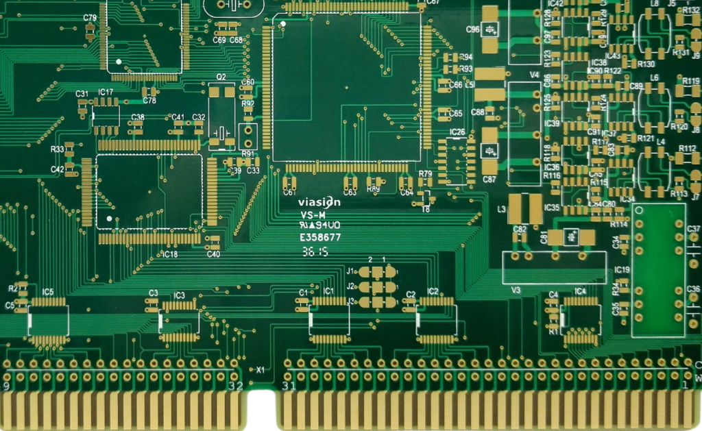
For modern electronic products, the complexity of PCB manufacturing continues to increase. HDI PCB, high-speed PCB, high-frequency PCB, rigid-flex PCB, heavy-copper PCB, and high-density multilayer PCB technologies all require more advanced manufacturing capabilities and tighter process control.
For engineers, understanding the PCB manufacturing process is more than learning how boards are physically produced. It provides practical knowledge that can improve PCB design, reduce manufacturing risks, improve first-pass yield, shorten development cycles, and control production costs.
Kingda combines PCB fabrication, PCB assembly, component procurement, engineering support, inspection, and testing into a one-stop manufacturing model. Its published capabilities cover standard and advanced multilayer PCB technologies, HDI, high-frequency, high-TG, thick-copper, rigid-flex, and other specialized PCB structures, providing a manufacturing pathway from prototype to production. (Kingda)