In the rapidly evolving electronics industry, products are becoming smaller, smarter, and more powerful. Technologies such as artificial intelligence, wireless communication, machine learning, IoT, automotive electronics, medical systems, and industrial automation are accelerating demand for reliable electronic hardware.
At the center of these products is the printed circuit board assembly (PCBA). A bare PCB provides the physical and electrical foundation, while PCB assembly transforms that board into a functional electronic circuit by mounting and soldering electronic components.
From smartphones and communication equipment to medical devices, automotive control systems, industrial controllers, and AI hardware, the quality of PCB assembly manufacturing directly influences product performance, reliability, service life, and production cost.
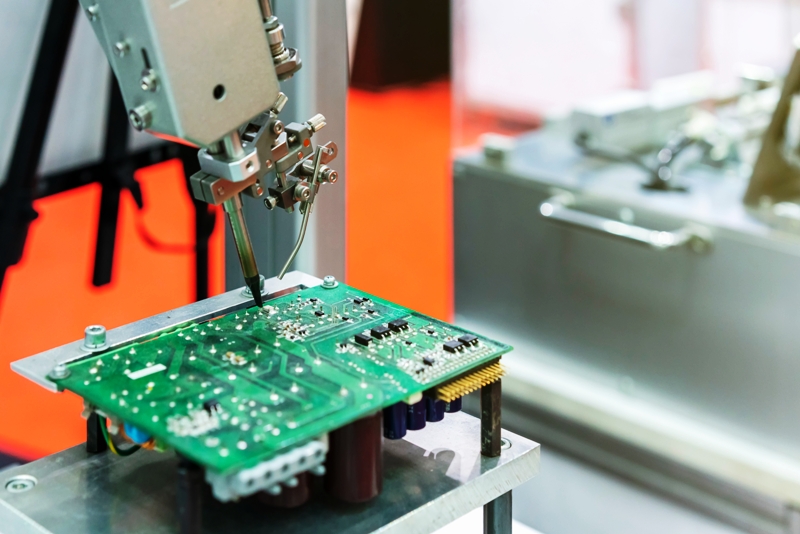
This guide explains what PCB assembly is, the differences between SMT and THT assembly, the major PCB assembly process steps, common soldering defects, quality-control methods, and the factors engineers should consider when choosing a reliable PCB assembly manufacturer.
What Is PCB Assembly?
PCB assembly, also known as PCBA manufacturing or printed circuit board assembly, is the process of mounting electronic components onto a bare printed circuit board and permanently connecting them through soldering or other approved interconnection methods.
The bare PCB contains conductive copper traces, pads, vias, and insulating materials, but it cannot perform the intended electronic function until components are installed.
Typical components mounted during PCB assembly include:
- Resistors
- Capacitors
- Inductors
- Diodes
- Transistors
- Integrated circuits
- Microcontrollers
- Connectors
- Relays
- Sensors
- Power devices
Electronic components can generally be classified as passive components, active components, and electromechanical components.
A passive component, such as a resistor or capacitor, does not provide power gain. Active components, such as transistors and ICs, can control, amplify, switch, or process electrical signals. Electromechanical components, including connectors, switches, and relays, combine electrical and mechanical functions.
Modern PCB assembly services use highly automated equipment to achieve consistent placement accuracy and soldering quality. Manual assembly remains useful for prototypes, specialized components, rework, and certain through-hole applications.
The two major assembly technologies are Surface Mount Technology (SMT) and Through-Hole Technology (THT).
SMT vs. THT PCB Assembly
Choosing between SMT PCB assembly, THT PCB assembly, or mixed technology depends on the electrical, mechanical, thermal, and manufacturing requirements of the product.
Through-Hole Technology (THT)
Through-Hole Technology, also called THT assembly, installs components by inserting their leads through drilled holes in the PCB.
The component leads are then soldered to copper pads, generally on the opposite side of the board.
Common through-hole components include:
- Large connectors
- Transformers
- Relays
- Large capacitors
- Power components
- Mechanical switches
- Certain inductors
THT remains valuable in applications where mechanical strength and component durability are particularly important.
Advantages of THT Assembly
High Mechanical Strength
Because component leads pass through the PCB, the resulting connection can provide strong mechanical retention. This makes THT suitable for products exposed to vibration, shock, or repeated mechanical stress.
Easy Repair and Rework
Larger through-hole components can often be manually removed, inspected, and replaced more easily than miniature SMT components.
High Power Handling
Many large power components are available in through-hole packages, making THT useful for power electronics and applications requiring higher current capacity.
Long-Term Durability
The mechanical connection between the component and board can provide excellent resistance to vibration and mechanical stress when appropriately designed and soldered.
Surface Mount Technology (SMT)
Surface Mount Technology, or SMT PCB assembly, mounts components directly onto copper pads on the PCB surface.
Unlike THT components, SMT components normally do not require component leads to pass through drilled holes.
SMT has become the dominant technology for modern electronics because it supports highly automated production and very high component density.
Advantages of SMT Assembly
Smaller and Lighter Products
SMT packages can be considerably smaller than traditional through-hole components, allowing designers to reduce PCB size and overall product dimensions.
High Component Density
SMT allows components to be installed closely together and can support components on both sides of the PCB.
High Production Efficiency
Automated solder paste printers, pick-and-place machines, reflow ovens, AOI systems, and other equipment make SMT highly suitable for automated production.
Excellent High-Speed Performance
Shorter interconnections and smaller packages can benefit high-frequency and high-speed circuit designs when combined with appropriate PCB layout and signal-integrity practices.
Lower Assembly Cost at Scale
Automation and high placement density can reduce production labor and improve manufacturing efficiency, particularly for medium- and high-volume programs.
Mixed Technology PCB Assembly
Many modern products require both SMT and THT.
A mixed technology PCB assembly may use SMT for small ICs, resistors, and capacitors while using THT for connectors, transformers, relays, or mechanically stressed components.
This approach allows engineers to optimize both electrical performance and mechanical reliability.
Kingda provides SMT, THT, and mixed-technology PCB assembly for prototype, low-volume, medium-volume, and high-volume requirements. Its published capabilities include automated solder paste printing, precision component placement, reflow soldering, wave/selective soldering, AOI, X-ray, ICT, and functional testing. (Kingda)
PCB Assembly Process: Step by Step
A typical PCB assembly process consists of several controlled stages.
PCB Design Review → BOM Verification → Solder Paste Printing → SPI → Component Placement → Reflow Soldering → AOI → THT Assembly → X-Ray/ICT/FCT → Final Inspection
The exact sequence depends on the board structure and assembly requirements.
1. Design and DFM Review
Before assembly begins, the manufacturer reviews the customer’s design data.
Typical inputs include:
- Gerber files
- BOM
- Pick-and-place/Centroid files
- Assembly drawings
- PCB stackup
- Special process requirements
- Testing requirements
A professional DFM (Design for Manufacturing) and DFA (Design for Assembly) review can identify issues such as:
- Incorrect footprints
- Insufficient component spacing
- Polarity errors
- Inadequate solder-mask clearance
- Difficult-to-assemble components
- BOM and placement-data mismatches
- Component availability problems
Early engineering review reduces the risk of assembly defects and expensive redesigns.
Kingda states that its engineering team performs DFM checks and verifies BOM and Gerber information before production. (Kingda)
2. Solder Paste Printing
For SMT assembly, solder paste is first deposited onto the PCB pads.
A stainless-steel stencil contains precisely defined apertures corresponding to the required solder pads.
A squeegee moves across the stencil, forcing solder paste through the apertures and onto the PCB.
The quality of this stage is critical because solder-paste volume and position directly influence solder-joint quality.
Important process parameters include:
- Stencil thickness
- Aperture size
- Solder paste type
- Squeegee pressure
- Printing speed
- Board support
- Stencil alignment
For lead-free manufacturing, SAC-based solder alloys are widely used.
3. Solder Paste Inspection
SPI (Solder Paste Inspection) uses automated optical systems to measure solder-paste deposition.
SPI can identify:
- Insufficient solder paste
- Excess solder paste
- Offset deposits
- Missing deposits
- Abnormal paste volume
Detecting solder-paste problems before component placement helps prevent downstream defects.
Kingda’s published quality-control flow includes 3D SPI before SMT/THT assembly, followed by AOI, X-ray, ICT/FCT, and final inspection. (Kingda)
4. Component Placement
Once the solder paste has been printed, high-speed pick-and-place machines position SMT components onto the PCB.
The machine reads placement data and uses vision systems to verify:
- Component identity
- Position
- Orientation
- Alignment
- PCB fiducials
Modern equipment can handle highly miniaturized packages, including fine-pitch ICs and miniature passive components.
Kingda’s published SMT capabilities include 01005 and 0201 passive components, fine-pitch devices, and BGA packages down to 0.35 mm pitch in its assembly services; its rapid-prototyping page separately lists 0.25 mm BGA capability. (Kingda)
5. Reflow Soldering
After placement, the PCB passes through a temperature-controlled reflow soldering oven.
The solder paste follows a carefully controlled thermal profile:
Preheat → Soak → Reflow → Cooling
During the reflow stage, solder melts and creates permanent electrical and mechanical connections between the components and PCB pads.
The thermal profile must be optimized to avoid:
- Cold solder joints
- Insufficient wetting
- Tombstoning
- Solder bridging
- Component overheating
- PCB warpage
Kingda states that its SMT production uses temperature-controlled reflow equipment, including 12-zone reflow ovens, to maintain soldering-process consistency. (Kingda)
6. Automated Optical Inspection
After reflow, AOI (Automated Optical Inspection) checks the assembled PCB.
AOI systems can detect:
- Missing components
- Wrong components
- Component misalignment
- Polarity errors
- Solder bridges
- Tombstoning
- Visible solder defects
AOI provides rapid and repeatable inspection and is especially valuable for larger production volumes.
7. THT Component Assembly
If the product contains through-hole components, THT assembly is performed after or during the SMT process according to the manufacturing strategy.
Depending on the design, manufacturers may use:
- Manual insertion
- Automated insertion
- Wave soldering
- Selective soldering
Selective soldering can be particularly useful for mixed SMT/THT assemblies because it selectively applies heat and solder to through-hole connections without unnecessarily exposing the complete board to a solder wave.
8. X-Ray Inspection
Certain solder joints cannot be inspected effectively from the PCB surface.
This is especially true for:
- BGA
- QFN
- LGA
- CSP
- Bottom-terminated components
X-ray inspection allows manufacturers to inspect hidden solder joints and identify:
- Voids
- Insufficient solder
- Bridging
- Misalignment
- Open joints
Kingda lists X-ray inspection among its standard inspection capabilities for complex PCB assemblies. (Kingda)
9. Electrical and Functional Testing
After assembly, the PCBA may undergo electrical and functional testing.
ICT
In-Circuit Testing (ICT) uses a fixture to check electrical characteristics and connectivity.
Typical checks may include:
- Resistance
- Capacitance
- Continuity
- Shorts
- Opens
- Selected component parameters
Flying Probe Testing
Flying probe testing uses moving probes and is often suitable for prototypes and low-volume production because it generally requires less dedicated tooling than ICT.
Functional Testing
Functional testing (FCT) evaluates the completed PCBA under operating conditions.
Depending on the product, tests may verify:
- Power input/output
- Communication interfaces
- Sensor operation
- Display functions
- Motor control
- RF functions
- Firmware operation
Kingda lists ICT, FCT, FAI, AOI, X-ray, and other inspection/testing capabilities as part of its quality-control system. (Kingda)
Key Considerations in PCB Assembly
1. Component Availability
Component shortages can delay an otherwise-ready PCB assembly project.
Factors affecting availability include:
- Manufacturer lifecycle status
- Lead time
- Global supply conditions
- Allocation
- Supplier reliability
- Minimum order quantities
A strong PCB assembly manufacturer should be able to identify sourcing risks early and recommend approved alternatives where appropriate.
Kingda states that it works with component distribution networks including Digi-Key, Mouser, and Element14 and provides component analysis, selection, and procurement support. (Kingda)
2. Material and Component Quality
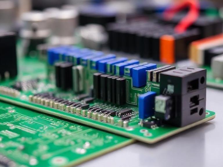
Component authenticity is especially important for automotive, medical, industrial, aerospace, and other reliability-sensitive products.
Effective controls include:
- Approved supplier management
- Incoming inspection
- Lot traceability
- BOM verification
- Date-code management
- Component documentation
Kingda describes incoming material verification, BOM validation, manufacturing traceability, and production records as part of its quality system. (Kingda)
3. Manufacturing Quality Control
Every major manufacturing stage should have appropriate process controls.
A typical quality flow may be:
IQC → SPI → SMT/THT → AOI → X-Ray → ICT/FCT → OQC
This approach allows manufacturing defects to be identified earlier instead of waiting until the final stage.
4. Production Capacity
Capacity should match the customer’s requirements.
Prototype projects require flexibility and rapid response, while mass production requires:
- Stable production lines
- High throughput
- Automated inspection
- Reliable component supply
- Traceability
- Process consistency
Kingda states that it supports prototype through volume production and operates multiple automated SMT production lines. (Kingda)
Common PCB Assembly Defects and Solutions
Solder Bridging
Solder bridging occurs when molten solder connects adjacent pads or pins, creating an unintended electrical short.
Common Causes
- Excessive solder paste
- Incorrect stencil aperture design
- Component misalignment
- Incorrect reflow profile
- Excessive pad density
Solutions
Manufacturers can reduce solder bridging through:
- Optimized stencil design
- Correct solder-paste volume
- Accurate component placement
- Controlled reflow profiles
- SPI and AOI inspection
Component Misalignment
Component misalignment may occur during placement or reflow.
Possible causes include:
- Incorrect placement coordinates
- Poor PCB fiducial recognition
- Improper solder-paste deposition
- Component movement during reflow
Solutions
Use:
- Accurate pick-and-place programming
- Vision alignment
- Consistent solder-paste deposition
- Proper thermal profiling
- SPI and AOI inspection
De-Wetting
De-wetting occurs when molten solder fails to spread properly across the pad or component termination.
Potential causes include:
- Oxidized surfaces
- Contamination
- Incorrect solder-paste storage
- Inadequate reflow conditions
Solutions
Maintain:
- Proper PCB cleanliness
- Correct solder-paste storage conditions
- Controlled paste shelf life
- Appropriate reflow parameters
- Suitable surface finishes
Tombstoning
Tombstoning occurs when a small passive component lifts onto one end during reflow.
It is often associated with uneven solder wetting or thermal imbalance between the two ends of the component.
Solutions
Manufacturers can reduce tombstoning through:
- Balanced solder-paste deposition
- Optimized pad design
- Proper component placement
- Controlled thermal profiles
- Uniform PCB heating
How to Improve PCB Assembly Quality
A reliable PCBA manufacturing process depends on more than automated machines. It requires coordinated engineering, process control, inspection, sourcing, and testing.
Design for Manufacturability
Design PCBs according to the actual capabilities of the manufacturing line.
Design for Assembly
Optimize component placement, spacing, polarity markings, package selection, and assembly orientation.
Component Lifecycle Management
Avoid relying exclusively on components that may soon become obsolete or difficult to source.
Automated Inspection
Use SPI, AOI, and X-ray where appropriate rather than relying exclusively on final manual inspection.
Testing Strategy
Define ICT, FCT, environmental testing, and other requirements during the development stage.
Traceability
Maintain records linking components, production batches, inspection results, and test outcomes to improve quality analysis and after-sales support.
Why Choose Kingda as Your PCB Assembly Partner?
For companies looking for a reliable PCB assembly manufacturer, selecting a partner with integrated fabrication, assembly, testing, sourcing, and engineering capabilities can simplify the overall supply chain.
Kingda is a Shenzhen-based one-stop PCBA manufacturer founded in 2013. Its published services cover PCB fabrication, component procurement, SMT, DIP/THT, testing, finished-product assembly, and box-build services. (Kingda)
One-Stop PCB and PCBA Services
Kingda integrates:
PCB Design → PCB Manufacturing → Component Procurement → SMT/THT Assembly → Testing → Finished Product Assembly
This reduces the need to coordinate multiple manufacturing suppliers and provides a single engineering and production workflow. (Kingda)
Advanced SMT and THT Capabilities
Kingda supports:
- SMT assembly
- THT assembly
- Mixed-technology assembly
- BGA
- QFN
- QFP
- Fine-pitch components
- 01005/0201 components
- Wave soldering
- Selective soldering
- Lead-free/RoHS assembly
Its published SMT operation includes 8 fully automated SMT lines and automated inspection systems including 3D SPI, AOI, and X-ray. (Kingda)
Comprehensive Inspection and Testing
Kingda’s quality-control system includes:
- 3D SPI
- AOI
- X-ray
- FAI
- ICT
- FCT
- Customized testing
This multi-stage approach helps identify defects before finished assemblies are released. (Kingda)
Flexible Production
Kingda states that it supports prototype, low-volume, medium-to-high-volume, and volume-production requirements. Its published prototype service supports no-MOQ projects and rapid turnaround, subject to project specifications and component availability. (Kingda)
Engineering Support
Kingda provides engineering support including:
- DFM
- DFA
- BOM analysis
- Component selection
- Component sourcing
- Production process optimization
- Testing support
This engineering involvement helps reduce design-related production risks before manufacturing begins. (Kingda)
International Quality Certifications
Kingda states that it holds ISO 9001, ISO 13485, IATF 16949, ISO 14001, and UL certification, and is an IPC member. These systems support projects with demanding quality requirements, particularly in automotive, medical, industrial, and other regulated applications. (Kingda)
Supply Chain and Traceability
Kingda reports component sourcing relationships with major distributors and maintains manufacturing traceability from incoming materials through final shipment. This helps customers manage component authenticity, production records, quality data, and product lifecycle requirements. (Kingda)
Conclusion
PCB assembly is the critical manufacturing stage that transforms a bare printed circuit board into a functional electronic assembly.
Modern PCBA manufacturing typically combines:
SMT + THT + Reflow Soldering + Wave/Selective Soldering + SPI + AOI + X-Ray + ICT/FCT
The correct assembly technology depends on the board’s component packages, electrical requirements, mechanical environment, production volume, and reliability requirements.
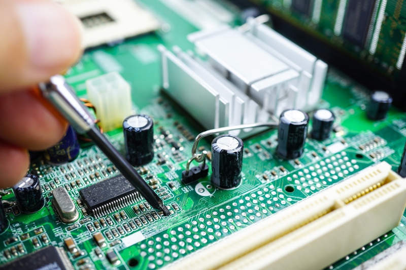
SMT provides high-density, automated assembly for modern compact electronics, while THT remains valuable for components requiring mechanical strength and higher-power connections. Mixed-technology assembly provides a practical solution when both technologies are required.
At the same time, successful PCB assembly depends on much more than placement and soldering. Component sourcing, DFM/DFA, process control, inspection, testing, traceability, and engineering support all contribute to the final quality of the product.
Kingda combines PCB fabrication, component procurement, SMT/THT assembly, inspection, testing, and finished-product integration within a one-stop manufacturing model. With its engineering support, automated production capabilities, comprehensive inspection systems, and quality-management certifications, Kingda can support projects from PCB prototyping through volume production. (Kingda)