Printed circuit boards (PCBs) are fundamental to almost every modern electronic product. From smartphones and computers to medical equipment, automotive systems, industrial controllers, telecommunications equipment, and AI hardware, PCBs provide the physical platform for electronic components while creating the conductive pathways that allow those components to communicate and operate together.
As electronics continue to become smaller, faster, more powerful, and more connected, PCB manufacturing is also becoming increasingly sophisticated. Modern circuit boards may require multilayer structures, fine-line circuitry, controlled impedance, HDI microvias, advanced materials, thermal-management structures, and highly automated inspection processes.
Understanding the PCB manufacturing process is therefore valuable not only for PCB manufacturers but also for hardware engineers, product developers, procurement teams, and OEMs. A clear understanding of fabrication helps designers make better material choices, improve manufacturability, reduce production risks, and achieve a smoother transition from prototype to mass production.
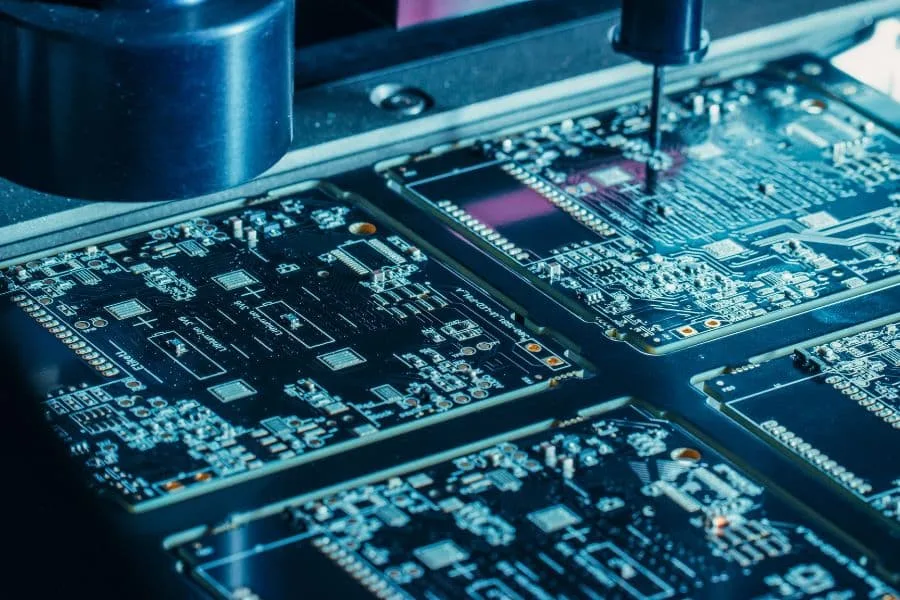
This guide provides a comprehensive overview of the PCB fabrication process, covering everything from PCB design and material selection to inner-layer fabrication, lamination, drilling, plating, solder mask, surface finishing, PCB assembly, inspection, and testing.
What Is PCB Manufacturing?
PCB manufacturing is the process of converting a digital circuit-board design into a physical printed circuit board.
The manufacturing process typically begins with design files such as Gerber, ODB++, or IPC-2581 and ends with a finished bare PCB that is electrically tested and ready for component assembly.
A typical PCB manufacturing process includes:
PCB Design → DFM Review → Material Preparation → Inner-Layer Fabrication → Lamination → Drilling → Copper Plating → Outer-Layer Imaging → Etching → Solder Mask → Surface Finish → Silkscreen → Electrical Testing → Final Inspection
For assembled products, another manufacturing stage follows:
PCB Fabrication → Component Sourcing → SMT/THT Assembly → Inspection → Functional Testing → Final Product Integration
The exact process varies according to the PCB structure, material, layer count, production volume, and application requirements.
Understanding PCB Design Before Manufacturing
Before a PCB enters a factory, it begins as an electronic design.
Engineers generally use EDA/CAD software such as Altium Designer, KiCad, Cadence, and other professional PCB design platforms to create schematics and PCB layouts.
The PCB design defines how components and conductive structures will interact.
Key design parameters include:
Trace Width
Trace width determines the physical width of copper conductors. It affects current-carrying capability, impedance, temperature rise, and manufacturability.
Trace Spacing
Trace spacing is the distance between conductive features. Adequate spacing reduces the risk of electrical shorts and supports manufacturing reliability.
Layer Count
The required number of layers depends on circuit complexity, routing density, power distribution, signal integrity, and mechanical constraints.
Via Structure
Designers may use:
- Through vias
- Blind vias
- Buried vias
- Microvias
- Stacked microvias
- Staggered microvias
Advanced via structures are especially important in HDI PCB manufacturing.
Stackup Design
A multilayer PCB stackup determines the arrangement of copper layers, dielectric materials, prepreg, and core materials. For high-speed or RF designs, stackup selection also determines controlled-impedance performance.
Thermal Management
Power electronics and high-density products may require:
- Thermal vias
- Heavy copper
- Copper planes
- Metal-core substrates
- Heat-spreading structures
A well-designed PCB should not only work electrically but also be practical to fabricate and assemble.
PCB Material Selection
Material selection has a direct impact on the electrical, thermal, mechanical, and environmental performance of a PCB.
FR-4
FR-4 is one of the most widely used PCB substrate materials. It combines good electrical insulation, mechanical strength, manufacturability, and cost efficiency.
Different FR-4 grades can provide different thermal characteristics, including higher Tg versions for applications exposed to elevated temperatures.
High-Tg Materials
High-Tg PCB materials provide improved thermal stability and dimensional control compared with standard materials.
They are commonly used in:
- Automotive electronics
- Industrial controls
- Power electronics
- High-reliability equipment
High-Frequency Materials
RF, microwave, radar, 5G, and high-speed digital applications may require specialized low-loss laminates.
Material selection should consider:
- Dielectric constant
- Dissipation factor
- Thermal expansion
- Moisture absorption
- Signal-loss characteristics
Copper
Copper forms the conductive circuitry of the PCB. Copper thickness is selected according to current requirements, thermal performance, impedance, and mechanical considerations.
Solder Mask
The solder mask is a protective polymer coating applied over most exposed copper. It prevents unintended solder connections while protecting the circuitry from oxidation, contamination, and environmental exposure.
Step-by-Step PCB Manufacturing Process
Step 1: Design Preparation and Pre-Production Engineering
The PCB fabrication process begins with engineering review.
Customers typically provide:
- Gerber files
- ODB++ or IPC-2581 files
- NC drill files
- PCB fabrication drawings
- Stackup specifications
- Material requirements
- Copper thickness
- Surface finish requirements
- Impedance specifications
- Panelization requirements
The manufacturer’s engineering team reviews the design before production.
DFM Analysis
A DFM (Design for Manufacturability) review may evaluate:
- Minimum trace width
- Minimum spacing
- Drill diameter
- Annular ring
- Copper-to-edge clearance
- Solder-mask clearance
- Layer registration
- Aspect ratio
- Impedance requirements
- Material availability
Early DFM analysis can identify issues before they become expensive production problems.
CAM Engineering
CAM engineers convert design information into manufacturing data used by fabrication equipment.
This can include:
- LDI data
- CNC drilling programs
- Routing programs
- Electrical test data
- Solder-mask artwork
- Silkscreen artwork
- Tooling holes
- Fiducials
- Test coupons
- Panelization data
This front-end engineering stage is one of the most important parts of modern PCB manufacturing because it creates the manufacturing instructions that control the rest of the process.
Step 2: Inner-Layer Fabrication
For a multilayer PCB, the internal copper layers are generally manufactured before the board is laminated.
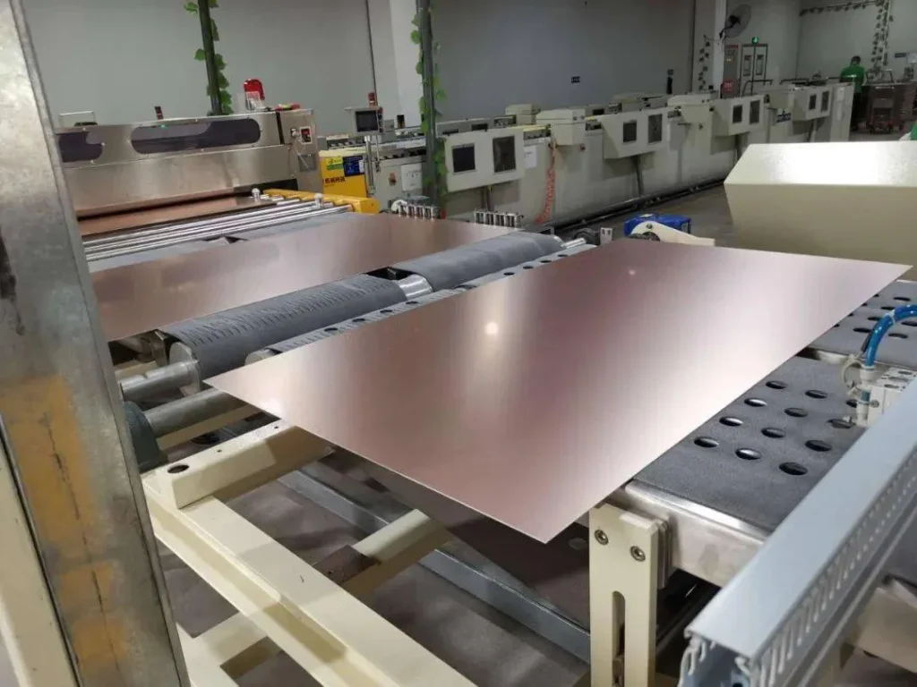
Copper-Clad Laminate Preparation
Copper-clad cores are cleaned to remove:
- Oxidation
- Dust
- Oil
- Fingerprints
- Other surface contamination
Proper surface preparation improves photoresist adhesion and image quality.
Photoresist Application
A photosensitive dry-film resist is laminated onto the copper surface.
The resist will later be selectively exposed to form the required circuit pattern.
Laser Direct Imaging
Modern PCB manufacturers increasingly use Laser Direct Imaging (LDI) for precise circuit imaging.
LDI transfers the digital manufacturing pattern directly onto the photoresist without relying on conventional phototools.
This technology supports:
- Fine lines
- Fine spacing
- Precise registration
- High-density circuitry
- Repeatable production
Developing and Etching
After imaging, the exposed panel undergoes development.
The unwanted photoresist is removed, exposing the copper areas that need to be etched.
Chemical etching removes unwanted copper, leaving behind the desired circuit pattern.
Inner-Layer AOI
After etching, Automated Optical Inspection (AOI) checks the completed inner-layer circuitry.
AOI can identify defects such as:
- Opens
- Shorts
- Missing copper
- Over-etching
- Under-etching
- Pattern distortion
- Registration errors
Defects are much easier to correct before lamination than after the layers have been permanently bonded together.
Step 3: Layer Bonding and Lamination
After all inner layers pass inspection, they are stacked and laminated.
A multilayer PCB usually contains:
Copper Layer + Core + Prepreg + Copper Layer + Prepreg + Copper Layer
depending on the required stackup.
Layer Alignment
Each inner-layer core must be accurately aligned.
Improper registration can cause:
- Pad misalignment
- Annular-ring violations
- Via connection problems
- Signal-integrity problems
Optical registration systems and tooling systems help maintain accurate layer alignment.
Lamination
The assembled stack is placed inside a lamination press.
Controlled:
- Temperature
- Pressure
- Vacuum
- Heating rate
- Cooling rate
are used to cure the prepreg resin and bond the individual layers into a single rigid PCB structure.
Proper lamination is essential for preventing:
- Delamination
- Voids
- Resin starvation
- Layer shifting
- Dimensional instability
The laminated panel is then cooled under controlled conditions before proceeding to drilling.
Step 4: PCB Drilling
After lamination, the PCB must be drilled to create electrical and mechanical holes.
Mechanical Drilling
CNC drilling machines create:
- Through-holes
- Component holes
- Plated holes
- Mounting holes
- Tooling holes
High-speed carbide drills are commonly used for standard PCB drilling.
Precise drilling is essential because the drill locations must align with the internal copper structures created during earlier manufacturing stages.
Laser Drilling
For HDI PCBs, laser drilling is used to produce microvias.
Microvias allow designers to create high-density interconnections while occupying less routing space than traditional through-hole structures.
Depending on the material and required feature size, manufacturers may use:
- CO₂ lasers
- UV lasers
Advanced PCB fabrication can combine different laser technologies to achieve the desired microvia structures.
Step 5: Hole Preparation and Copper Plating
After drilling, the holes contain resin residue and drilling debris.
These contaminants must be removed before plating.
Deburring and Desmear
Deburring removes unwanted mechanical material around the drilled holes.
Desmear removes epoxy resin that may cover exposed internal copper.
Without proper desmear, the plated hole may not form a reliable electrical connection to internal layers.
Electroless Copper
An electroless copper process deposits a thin conductive copper layer throughout the hole walls.
This creates the conductive foundation required for subsequent electrolytic copper plating.
Electrolytic Copper Plating
The panels are placed into an electroplating bath.
Electrical current deposits additional copper onto:
- Hole walls
- Outer-layer copper
- Pads
- Circuit features
The final copper thickness must meet the requirements defined by the design and applicable manufacturing standards.
Step 6: Outer-Layer Imaging and Etching
Once the holes are plated, the outer circuitry is created.
Outer-Layer Imaging
The outer copper surfaces are coated with photoresist and exposed using the PCB manufacturing data.
Pattern Plating
Copper is plated onto areas that form the final circuitry and plated holes.
This simultaneously increases copper thickness on the outer circuitry and inside plated through-holes.
Tin Plating
Tin may be used as an etch resist to protect the completed circuit pattern during the subsequent etching stage.
Etching
Unwanted copper is chemically removed.
The result is the finished outer-layer circuit pattern, including:
- Signal traces
- Pads
- Ground planes
- Power planes
- Plated through-holes
Step 7: Solder Mask Application
The PCB then receives its protective solder mask.
Most modern manufacturers use Liquid Photoimageable (LPI) solder mask.
The solder mask protects copper traces while leaving solderable pads exposed.
Its major functions include:
- Preventing solder bridges
- Protecting copper
- Reducing oxidation
- Improving electrical insulation
- Increasing environmental resistance
Although green is the most common solder-mask color, manufacturers can also provide other colors depending on customer requirements.
Step 8: Silkscreen Application
The PCB silkscreen provides visual information used during manufacturing, assembly, testing, and repair.
It may include:
- Component reference designators
- Polarity markings
- Pin-1 indicators
- Logos
- Revision numbers
- Warning labels
Modern production commonly uses inkjet-based legend printing for high-resolution markings.
Step 9: Surface Finishing
The exposed copper pads require a PCB surface finish to prevent oxidation and maintain solderability.
Common surface finishes include:
HASL
Hot Air Solder Leveling (HASL) is cost-effective and widely used for general applications.
ENIG
Electroless Nickel Immersion Gold (ENIG) provides a flat surface suitable for fine-pitch SMT and BGA applications.
OSP
Organic Solderability Preservative (OSP) provides a thin protective coating while maintaining a relatively flat pad surface.
Immersion Silver
Immersion silver provides good solderability and is suitable for selected high-density applications.
ENEPIG
ENEPIG provides a highly reliable surface finish for demanding applications involving fine-pitch components and complex assembly requirements.
The correct surface finish depends on:
- PCB application
- Assembly technology
- Required shelf life
- Reliability requirements
- Cost
- Environmental conditions
Step 10: Electrical Testing and Inspection
After fabrication, finished boards undergo inspection and electrical testing.
Flying Probe Testing
Flying-probe systems are particularly useful for prototype and low-volume PCB production because they do not require expensive dedicated fixtures.
Bed-of-Nails Testing
High-volume PCB manufacturing often uses bed-of-nails fixtures.
These fixtures allow rapid electrical verification of many test points simultaneously.
Electrical testing can identify:
- Opens
- Shorts
- Incorrect connections
- Electrical isolation failures
Impedance Testing
For high-speed and RF PCBs, impedance testing verifies that transmission lines meet specified electrical characteristics.
Test coupons may be incorporated into the production panel to support impedance verification.
Visual Inspection
Final visual inspection checks:
- Surface finish
- Solder mask
- Silkscreen
- Board dimensions
- Edge quality
- Drilling
- Copper features
- General workmanship
Step 11: PCB Depanelization and Final Inspection
PCBs are often manufactured in panels to improve material utilization and production efficiency.
After fabrication and testing, individual boards may be separated using:
- CNC routing
- V-scoring
- Tab routing
- Punching
The selected method depends on board geometry and customer requirements.
Final inspection verifies that each board meets the specified:
- Dimensions
- Thickness
- Hole sizes
- Surface finish
- Copper thickness
- Solder-mask registration
- Electrical performance
Step 12: Packaging and Shipment
After passing inspection, bare PCBs are packaged for transportation.
Depending on product requirements, packaging may include:
- ESD-safe bags
- Moisture-barrier bags
- Desiccant
- Humidity indicator cards
- Protective separators
- Vacuum packaging
Correct packaging helps protect PCBs from moisture absorption, oxidation, contamination, physical impact, and electrostatic damage.
PCB Assembly After PCB Fabrication
PCB fabrication produces a bare circuit board. To create a functional electronic assembly, components must be installed.
The PCB assembly process typically includes:
Solder Paste Printing → SPI → Pick-and-Place → Reflow Soldering → AOI → X-Ray → THT Assembly → Functional Testing
Depending on the project, manufacturers may also provide:
- IC programming
- Conformal coating
- Wire harness assembly
- Cable assembly
- Box build assembly
- Burn-in testing
- Environmental testing
This is why choosing a manufacturer capable of both PCB fabrication and PCB assembly can simplify the manufacturing supply chain.
SMT Assembly
Surface Mount Technology (SMT) is widely used for modern PCB assembly.
Typical SMT processes include:
- Solder paste printing
- Solder paste inspection
- Component placement
- Reflow soldering
- AOI
- X-ray inspection where required
- Functional testing
SMT supports high component density, automated manufacturing, small packages, and high production efficiency.
Through-Hole Assembly
Through-hole components remain important for applications requiring:
- Mechanical strength
- High-current connections
- Large connectors
- Transformers
- Relays
- Power components
THT components can be assembled through:
- Manual insertion
- Automated insertion
- Wave soldering
- Selective soldering
Sustainability in PCB Manufacturing
Environmental considerations are becoming increasingly important in modern PCB fabrication.
Manufacturers are reducing environmental impact through:
Lead-Free Manufacturing
Lead-free solder and RoHS-compliant materials reduce the use of restricted substances in electronics.
More Efficient Production
Modern manufacturing equipment can reduce:
- Energy consumption
- Chemical consumption
- Material waste
- Production scrap
Waste Treatment
Responsible PCB manufacturers implement controlled treatment of wastewater, chemical waste, and production residues.
Longer Product Life
Higher manufacturing quality can also contribute to longer electronic product life, reducing replacement frequency and electronic waste.
Kingda states that its manufacturing operations incorporate environmental management practices and ISO 14001 certification, alongside its broader quality and manufacturing systems. (Kingda)
Why Choose Kingda for PCB Manufacturing?
Kingda provides an integrated PCB manufacturing and PCBA solution, combining PCB fabrication, component procurement, SMT assembly, DIP/THT assembly, testing, and final product integration. The company states that it was founded in 2013 and serves customers in areas including medical, automotive, industrial automation, AI, smart home, security, power, and communications. (Kingda)
Broad PCB Manufacturing Capabilities
Kingda’s published PCB manufacturing capabilities include:
- 1–48-layer PCB products
- Multilayer PCBs
- HDI PCBs
- High-TG thick-copper PCBs
- High-frequency PCBs
- Rogers mixed-lamination PCBs
- Blind and buried-via PCBs
- Metal-base PCBs
- Gold-finger PCBs
- Impedance-controlled PCBs
- High-frequency antenna PCBs
Its published capability tables also cover advanced features such as stacked microvias, copper-filled microvias, buried filled vias, and sequential build-up structures. (Kingda)
One-Stop PCB and PCBA Manufacturing
Instead of managing separate PCB fabrication, component procurement, assembly, and testing suppliers, Kingda integrates these processes into a single manufacturing workflow.
Its services include:
PCB Design → PCB Fabrication → Component Procurement → SMT → DIP/THT → Testing → Finished Product Assembly
This integrated structure can help reduce supplier handoffs and simplify project management. (Kingda)
Advanced PCB Assembly
Kingda states that its SMT manufacturing includes automated production lines and inspection technologies such as:
- 3D SPI
- AOI
- X-ray
- ICT
- FCT
- FAI
Its published SMT capabilities include BGA, QFN, QFP, CSP, PoP, 0201 components, and fine-pitch assembly. (Kingda)
Engineering and DFM Support
Kingda provides engineering support covering PCB design, DFM/DFA analysis, component sourcing, manufacturing review, and PCBA testing.
This helps engineers identify potential manufacturability issues before fabrication and assembly begin. (Kingda)
Quality Certifications
Kingda states that it has obtained:
- ISO 9001
- ISO 13485
- IATF 16949
- ISO 14001
- UL certification
- IPC membership
These quality systems support applications with demanding requirements, particularly medical, automotive, and industrial electronics. (Kingda)
Prototype to Mass Production
Kingda supports a manufacturing path from rapid PCBA prototyping and low-volume production to high-volume production. Its published rapid-prototyping information indicates prototype lead times can be approximately 2–3 days under suitable conditions, with expedited services available for some projects. (Kingda)
PCB Manufacturing Process: Key Factors Engineers Should Consider
Before sending a PCB design to production, engineers should evaluate five important areas.
1. Manufacturability
A PCB should be designed according to the manufacturer’s actual process capabilities.
2. Material Availability
Using readily available materials can reduce lead time and supply-chain risk.
3. Assembly Compatibility
Footprints, spacing, component packages, and solder-mask design should support the intended SMT/THT process.
4. Testing Strategy
Electrical and functional testing should be considered during design rather than added after fabrication.
5. Scalability
A good prototype design should have a realistic path toward low-volume PCB production and mass PCB manufacturing.
PCB Manufacturing Process FAQs
What is the PCB manufacturing process?
The PCB manufacturing process converts digital PCB design data into physical bare circuit boards through imaging, etching, lamination, drilling, plating, solder mask, surface finishing, testing, and inspection.
What is the most important PCB manufacturing step?
There is no single step that determines PCB quality. Front-end engineering, layer registration, lamination, drilling, copper plating, surface finishing, and electrical testing all contribute to final reliability.
What materials are commonly used in PCB manufacturing?
FR-4 is the most common material, while high-TG laminates, high-frequency materials, polyimide, metal-core substrates, and specialized laminates are used for demanding applications.
What is the difference between PCB fabrication and PCB assembly?
PCB fabrication produces the bare circuit board. PCB assembly (PCBA) installs electronic components onto the fabricated board.
How can PCB manufacturing lead time be reduced?
Lead time can often be reduced by:
- Using standard materials
- Simplifying unnecessary complexity
- Preparing complete manufacturing files
- Completing DFM early
- Confirming stackup requirements
- Using readily available materials
- Selecting an experienced PCB manufacturer
Conclusion
The PCB manufacturing process is a highly controlled sequence that transforms a digital PCB design into a reliable physical circuit board.
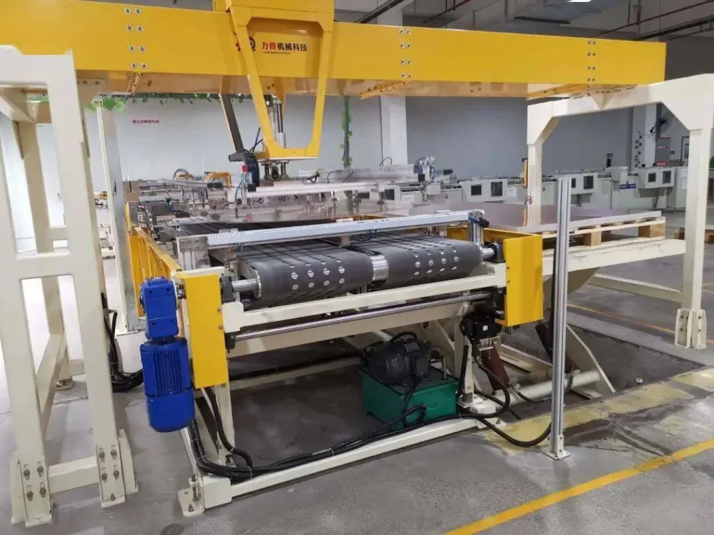
The core workflow can be summarized as:
PCB Design → DFM → Inner-Layer Fabrication → Lamination → Drilling → Copper Plating → Outer-Layer Processing → Solder Mask → Surface Finish → Testing → Inspection → Packaging
For multilayer, HDI, high-frequency, automotive, medical, and other high-reliability PCBs, every stage requires precise process control.
Understanding PCB fabrication allows engineers to make better decisions about materials, stackups, trace geometry, vias, thermal management, assembly, testing, and production scalability.
Kingda offers an integrated path from PCB design and fabrication to component sourcing, SMT/THT assembly, inspection, testing, and final product integration. With broad PCB fabrication capabilities, advanced PCBA equipment, engineering support, and internationally recognized quality systems, Kingda can support electronics projects from prototype development through production. (Kingda)