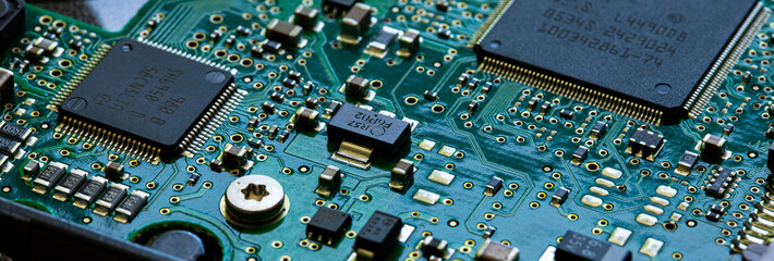
Quick Turn PCB Manufacturing for Fast Product Development
When electronic product development depends on speed, conventional PCB production schedules can become a major bottleneck. Quick turn PCB manufacturing is designed to shorten the time between design completion and receiving functional printed circuit boards, allowing engineers to validate designs, identify problems, and move toward production more efficiently.
A reliable quick turn PCB service combines fast engineering review, material availability, efficient manufacturing processes, automated inspection, and responsive logistics. Depending on board specifications, a manufacturer may support prototype quantities within a few days and transition successful designs into low-volume or mass production.
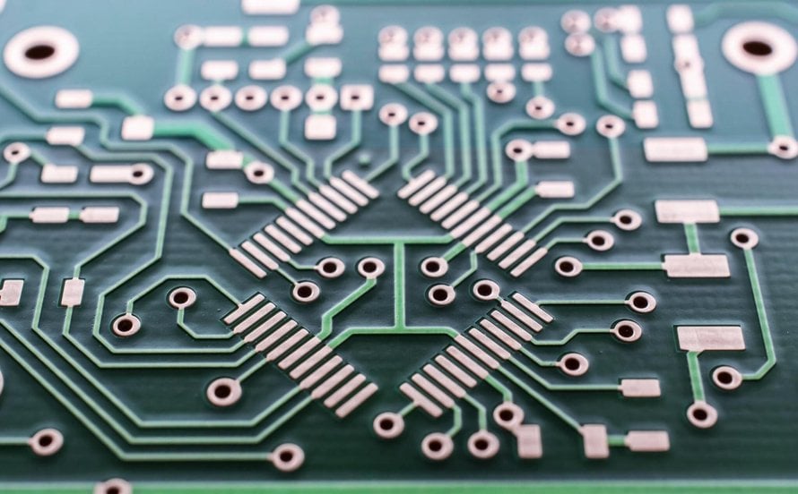
For customers who need a complete manufacturing solution, PCB manufacturing can cover everything from prototype fabrication to production-scale requirements.
What Is a Quick Turn PCB?
A quick turn PCB is a printed circuit board manufactured and delivered within a significantly shorter lead time than a conventional PCB production order.
The primary purpose of quick-turn manufacturing is to accelerate electronic product development. Instead of waiting several weeks for a prototype, engineering teams can receive boards quickly and use them for electrical testing, firmware development, mechanical verification, thermal evaluation, and functional validation.
Rapid PCB manufacturing is particularly valuable when a product is under active development and design revisions are expected. A shorter manufacturing cycle allows engineers to identify design problems earlier and make changes before committing to larger production quantities.
Quick-turn services can support a wide range of PCB technologies, including:
- Single-sided and double-sided PCBs
- Multilayer PCBs
- High-TG FR-4 PCBs
- High-speed and high-frequency PCBs
- HDI PCBs
- Flexible PCBs
- Rigid-flex PCBs
- Metal core PCBs
- Heavy copper PCBs
- Specialized material PCB designs
The actual lead time depends on board complexity, materials, layer count, copper weight, surface finish, quantity, testing requirements, and special manufacturing processes.
Why Quick Turn PCB Manufacturing Matters
The electronics market continues to move toward shorter development cycles. Consumer electronics, industrial controls, medical equipment, automotive electronics, communication systems, IoT devices, and other products often require multiple engineering iterations before entering production.
A PCB prototype manufacturing strategy based on fast turnaround can reduce waiting time between design revisions and improve the overall product development cycle.
Faster Design Verification
Engineers can quickly evaluate whether a PCB performs according to the original design. Problems involving signal integrity, power distribution, component placement, thermal performance, or mechanical integration can be identified earlier.
Shorter Product Development Cycles
Receiving prototype boards faster allows hardware, firmware, mechanical, and testing teams to work in parallel instead of waiting for PCB fabrication to finish.
Earlier Detection of Manufacturing Problems
DFM review and prototype production can expose issues involving trace spacing, via structures, component footprints, solder mask, drill sizes, or material selection before larger quantities are produced.
More Efficient Design Iteration
When prototype boards can be manufactured quickly, engineering teams have more opportunities to modify, test, and optimize the design before production release.
Faster Time to Market
A compressed PCB development cycle can help companies move validated electronic products toward market launch more quickly.
Applications of Quick Turn PCB Manufacturing
Quick turn PCB manufacturing can be used throughout the product development lifecycle rather than only for early prototypes.
PCB Prototyping
Prototype PCBs are typically produced in relatively small quantities for engineering verification. Fast production enables engineers to evaluate their designs without waiting for standard manufacturing lead times.
This approach is especially useful for products with aggressive development schedules or designs that are still undergoing frequent revisions.
Pre-Production Validation
After initial prototypes have passed functional testing, a larger pre-production batch can be manufactured to validate the design under conditions closer to actual production.
Pre-production testing can reveal issues that may not appear in a very small prototype sample. Manufacturing consistency, assembly performance, component availability, and production testing can all be evaluated at this stage.
Production Runs
Fast-turn PCB services can also be useful for production requirements when delivery time is critical. Once a design has been fully validated, the manufacturer can transition from prototype quantities to low-volume and larger production runs.
A complete PCB assembly capability can further simplify the transition by combining PCB fabrication with component placement, soldering, inspection, and testing.
Materials Available for Quick Turn PCBs
Material selection has a direct influence on electrical performance, thermal behavior, mechanical reliability, and manufacturing lead time.
Common materials used for rapid PCB manufacturing include:
FR-4
FR-4 remains one of the most widely used PCB materials because of its balanced electrical, mechanical, thermal, and cost characteristics. High-TG FR-4 can be selected for applications requiring improved thermal performance.
High-Speed Materials
High-speed digital designs require controlled electrical characteristics and stable dielectric properties. Specialized high-speed laminate materials may be used where signal integrity is critical.
High-Frequency Materials
RF and microwave applications may require low-loss materials with controlled dielectric properties. Material selection should be based on operating frequency, impedance requirements, thermal conditions, and application requirements.
Polyimide
Polyimide is commonly used for flexible circuits because of its flexibility and thermal performance.
Metal Core Materials
Aluminum and other metal-core PCB structures can improve heat dissipation and are frequently used in LED lighting, power electronics, and thermal-intensive applications.
Specialized Materials
Depending on the design, manufacturers may also support PTFE-based materials, ceramic materials, hybrid constructions, heavy copper structures, and other specialized PCB technologies.
Material availability should always be confirmed before requesting an accelerated production schedule because special materials may require longer procurement times.
PCB Manufacturing Capabilities for Quick Turn Projects
The manufacturing capability of the supplier is one of the most important factors affecting turnaround time.
A capable manufacturer should be able to manage engineering review, material preparation, fabrication, inspection, testing, and shipment within a coordinated production workflow.
Typical quick-turn capabilities may include:
- 1–100 layer PCB production depending on technology and supplier capability
- Controlled impedance PCB manufacturing
- Blind and buried vias
- Microvias
- Stacked and staggered vias
- Via-in-pad structures
- Back drilling
- Heavy copper PCB fabrication
- High-density interconnect technology
- Flexible and rigid-flex PCB fabrication
- High-frequency and high-speed PCB production
For more detailed technical specifications, the PCB capabilities page provides information on manufacturing tolerances, copper weights, HDI structures, dielectric thickness, microvia technology, and other production parameters.
Factors That Affect PCB Turnaround Time
Although a quick turn PCB manufacturer can significantly shorten production schedules, not every PCB can be manufactured within the same lead time. Several technical and logistical factors influence delivery.
Manufacturing Capacity
Production capacity is essential for accelerated PCB manufacturing. A supplier with sufficient equipment, engineering resources, production personnel, and backup capacity can respond more effectively to urgent orders.
Equipment and Automation
Modern drilling, imaging, plating, lamination, inspection, and testing equipment can improve manufacturing efficiency and consistency.
Automation is particularly important when a manufacturer needs to maintain short lead times while handling multiple projects simultaneously.
Material Availability
Material procurement can become a major constraint. Standard FR-4 materials may be readily available, while specialized high-frequency, high-speed, PTFE, ceramic, or hybrid materials may require additional sourcing time.
For an urgent PCB project, confirming material availability before production begins can prevent unnecessary delays.
PCB Design Complexity
Complex designs generally require more engineering and manufacturing steps.
For example, a high-layer-count HDI PCB with microvias, sequential lamination, fine-pitch features, and controlled impedance requirements will normally require more processing than a simple two-layer FR-4 board.
Layer Count
More PCB layers generally mean additional lamination and processing stages. Increasing layer count can therefore increase manufacturing time.
Via Structures
Blind vias, buried vias, microvias, stacked vias, and via-in-pad structures require additional manufacturing processes and tighter process control.
Special Processes
Special requirements such as back drilling, countersunk holes, peelable solder mask, hard gold, copper-filled vias, or other customized processes may extend the production schedule.
Quality Requirements
Inspection and testing requirements also affect lead time. Higher reliability applications may require additional electrical testing, dimensional inspection, AOI, X-ray inspection, or other quality-control procedures.
Quick Turn PCB Manufacturing Process
A reliable quick turn PCB process requires close coordination between engineering, procurement, manufacturing, inspection, and logistics.
Step 1: Design File Submission
The process begins when the customer submits the PCB design package.
Typical files may include:
- Gerber files
- NC drill files
- PCB fabrication drawings
- Stack-up information
- Material specifications
- Surface finish requirements
- Controlled impedance requirements
- Special process instructions
The manufacturer reviews the files to determine whether the design can be produced according to the requested specifications and delivery schedule.
Step 2: Engineering and DFM Review
Engineering teams review the design for potential manufacturing problems.
The review may examine:
- Trace width and spacing
- Pad dimensions
- Drill sizes
- Annular rings
- Copper distribution
- Layer stack-up
- Impedance requirements
- Via structures
- Solder mask clearance
- Board dimensions
- Manufacturing tolerances
Early DFM review can prevent production interruptions and reduce the risk of rework.
Step 3: Material Preparation
The required laminate, copper foil, prepreg, solder mask, surface-finish materials, and other production materials are prepared.
For urgent orders, material availability should be confirmed before the production schedule is finalized.
Step 4: Inner-Layer Imaging
For multilayer boards, the circuit pattern is transferred onto the inner copper layers using imaging technology.
The unwanted copper is subsequently removed through etching, leaving the required circuit pattern.
Step 5: Layer Lamination
The prepared inner layers are aligned with dielectric materials and copper foils before being laminated under controlled temperature and pressure.
This creates the multilayer PCB structure.
Step 6: Drilling
Mechanical or laser drilling is used to create through-holes, blind vias, buried vias, and microvias according to the design requirements.
High-density designs may require laser drilling and more advanced via processing.
Step 7: Copper Plating
Copper plating creates conductive connections between PCB layers through drilled holes and vias. Additional copper can also be deposited to achieve the specified conductor thickness.
Step 8: Outer-Layer Imaging and Etching
The outer-layer circuit pattern is created, unwanted copper is removed, and the final conductive pattern is formed.
Step 9: Solder Mask and Silkscreen
Solder mask is applied to protect exposed copper areas and help prevent solder bridges during assembly.
Silkscreen can then be applied to identify component locations, reference designators, polarity indicators, logos, and other information.
Step 10: Surface Finish
Exposed copper pads require a suitable surface finish to protect the copper and provide a reliable soldering surface.
Common PCB surface finishes include:
- HASL
- Lead-free HASL
- ENIG
- OSP
- ENEPIG
- Immersion tin
- Immersion silver
The appropriate finish depends on the application, assembly process, reliability requirements, and cost considerations.
Step 11: Inspection and Testing
Finished PCBs undergo quality inspection and electrical testing according to project requirements.
Inspection may include:
- Automated Optical Inspection (AOI)
- Electrical testing
- X-ray inspection
- Dimensional inspection
- Visual inspection
- Impedance testing
- Microsection analysis where required
For customers requiring assembled boards, turnkey PCB assembly can integrate PCB fabrication, component procurement, SMT assembly, through-hole assembly, inspection, testing, and final packaging.
Step 12: Packaging and Shipping
After final inspection, PCBs are packaged appropriately to protect them from moisture, contamination, physical damage, and electrostatic discharge.
Express logistics can then be selected according to the required delivery schedule and destination.
How to Choose a Quick Turn PCB Manufacturer
Choosing the right supplier is critical when delivery time and product reliability are equally important.
Evaluate Manufacturing Capabilities
Do not select a supplier based solely on advertised delivery time. Confirm that the manufacturer can actually produce your required layer count, material, copper thickness, via structure, board size, surface finish, and tolerance.
Check Engineering Support
Strong engineering support is particularly important for urgent PCB projects. An experienced engineering team can identify potential problems before production and help prevent avoidable delays.
Confirm Quality Management
A short delivery time should never come at the expense of PCB reliability. Review the manufacturer’s quality system, inspection capabilities, testing procedures, and relevant industry certifications.
Review Production Scalability
A supplier should ideally support the entire development cycle, from prototype to pre-production and volume manufacturing.
This avoids the need to transfer a validated design to a completely different supplier when production requirements increase.
Consider PCB Assembly Capability
For customers requiring completed electronic assemblies, a supplier offering both PCB fabrication and assembly can simplify procurement and project management.
The PCBA capabilities service covers a broad range of PCB assembly requirements, including different board types, component packages, assembly volumes, and manufacturing processes.
Evaluate Communication and Responsiveness
Fast PCB manufacturing requires fast communication. Engineering questions, quotation requests, material confirmation, design changes, and production updates should be handled promptly.
A responsive supplier can help prevent small issues from becoming major schedule problems.
Quick Turn PCB Manufacturing for Prototype Development
Prototype development is one of the strongest use cases for PCB prototype manufacturing.
A typical development cycle may include:
PCB Design → DFM Review → Prototype Fabrication → PCB Assembly → Functional Testing → Design Revision → Second Prototype → Pre-Production → Mass Production
Reducing the fabrication time between these stages can significantly accelerate product development.
For engineering teams that need assembled prototypes rather than bare boards, prototype PCB assembly provides a way to move from PCB fabrication to functional electronic testing more efficiently.
Quality Considerations for Fast PCB Production
Speed should not replace quality control.
A professional quick turn PCB manufacturer should maintain consistent process control throughout fabrication. Fast production should still include engineering verification, material control, process inspection, electrical testing, and final quality inspection.
Important quality considerations include:
- Correct material specification
- Controlled layer alignment
- Reliable copper plating
- Accurate drilling
- Proper solder mask registration
- Appropriate surface finish
- Controlled impedance where required
- Electrical continuity testing
- AOI inspection
- X-ray inspection for applicable designs
- Traceability and production documentation
The goal of quick-turn manufacturing is not simply to produce a PCB faster. The objective is to produce a functional, reliable PCB faster without compromising the requirements of the original design.
Quick Turn PCB vs. Standard PCB Manufacturing
The primary difference between conventional and quick-turn manufacturing is production priority and scheduling.
| Factor | Quick Turn PCB | Standard PCB Production |
|---|---|---|
| Lead Time | Shortened | Standard schedule |
| Typical Use | Prototypes and urgent projects | Planned production |
| Engineering Response | Fast | Standard |
| Material Planning | Priority-based | Normal procurement |
| Production Scheduling | Accelerated | Regular queue |
| Design Iteration | Faster | Slower |
| Cost | May be higher for urgent orders | Usually more economical |
| Best Application | Development and time-sensitive projects | Planned production |
Quick-turn manufacturing is therefore not necessarily the lowest-cost option. Its main value is reducing the time required to obtain usable boards.
How to Reduce PCB Manufacturing Lead Time
Customers can take several practical steps to make their PCB projects easier to manufacture quickly.
Provide Complete Design Files
Incomplete or inconsistent Gerber, drill, drawing, or BOM information can delay engineering review.
Use Standard Materials When Possible
Standard materials are generally easier to source than specialized materials and can help reduce procurement time.
Minimize Unnecessary Complexity
Avoiding unnecessarily complicated via structures, unusual board thicknesses, or special processes can make production faster.
Confirm Requirements Before Production
Clearly define the layer count, material, copper weight, surface finish, impedance requirements, testing requirements, and special processes before the order is released.
Respond Quickly to Engineering Questions
Fast communication between the customer and manufacturer can prevent engineering approvals from becoming the bottleneck.
Plan Shipping in Advance
Production completion is only one part of the delivery schedule. Selecting an appropriate logistics method in advance can help ensure the completed boards arrive when needed.
Conclusion
Quick turn PCB manufacturing provides an effective solution for companies that need to shorten electronic product development cycles. By combining engineering review, material planning, efficient PCB fabrication, automated inspection, electrical testing, and responsive logistics, manufacturers can deliver reliable boards in significantly less time than conventional production schedules.
The most important consideration is to balance speed with technical capability and quality. A supplier should be able to manufacture the required PCB technology, provide engineering support, maintain appropriate quality controls, and scale from prototype quantities to production volumes.
For engineers developing new electronic products, rapid PCB manufacturing can shorten the gap between design and physical validation. For companies preparing products for market, PCB prototype manufacturing can reduce iteration time and help identify potential problems before volume production.
Ultimately, selecting the right quick turn PCB manufacturer means choosing a partner that can deliver not only fast PCB fabrication, but also consistent quality, engineering expertise, flexible production capabilities, and dependable support throughout the product development cycle.