Low Loss PCB Manufacturing
16+ Years of PCB Manufacturing Experience
A Low Loss PCB is designed to minimize signal attenuation and transmission loss in high-speed and high-frequency electronic systems. Compared with conventional circuit boards, low-loss designs use specialized dielectric materials, precise impedance control, optimized copper structures, and advanced manufacturing processes to maintain signal integrity.
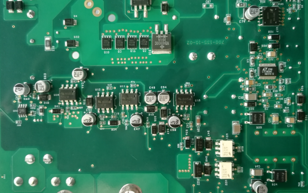
Typical applications include telecommunications, data centers, medical electronics, aerospace, automotive electronics, RF and microwave systems, networking equipment, and other high-speed electronic products.
GOPCBA supports advanced PCB manufacturing for complex electronic applications, including multilayer boards, high-frequency designs, HDI structures, controlled impedance boards, and specialized material combinations.
Key capabilities include:
- Materials: Enhanced FR-4, high-performance laminates, Rogers, PTFE, ceramic and other advanced dielectric materials
- Layer Count: Multilayer PCB manufacturing for complex designs
- PCB Structures: Blind vias, buried vias, microvias, and HDI
- Impedance Control: Tight control of single-ended and differential impedance
- Quality Control: Electrical testing, AOI, dimensional inspection, and process verification
What Is a Low Loss PCB?
A Low Loss PCB is a printed circuit board engineered to reduce electrical energy loss as high-speed or high-frequency signals travel through copper traces and dielectric materials.
At higher frequencies, signal loss becomes increasingly important. Dielectric loss, conductor loss, impedance discontinuities, surface roughness, trace geometry, and material variation can all affect transmission performance.
Low-loss PCB technology addresses these factors through carefully selected materials and controlled manufacturing processes. The objective is to preserve signal amplitude, reduce attenuation, minimize distortion, and maintain predictable electrical performance across the complete signal path.
This makes low-loss technology particularly valuable for systems where high data rates, long transmission paths, low latency, or stable RF performance are required.
Why Use Low Loss PCB Technology?
Maintaining High-Speed Signal Integrity
High-speed digital signals contain high-frequency components that can be significantly affected by dielectric and conductor losses. Excessive attenuation can reduce signal quality and create problems such as timing errors, eye closure, jitter, and increased bit-error rates.
A properly engineered Low Loss PCB reduces these losses and helps maintain signal quality throughout the transmission path.
Supporting High-Frequency Applications
RF and microwave circuits are highly sensitive to material properties, trace geometry, and impedance variation. For these applications, Low Loss PCB Materials with stable electrical characteristics can provide more predictable performance.
The combination of appropriate laminate selection, controlled impedance, and precision fabrication is essential for reliable high-frequency circuit performance.
Improving Energy Efficiency
Lower dielectric and conductor losses mean less signal energy is converted into heat during transmission. This can improve overall power efficiency, particularly in systems that continuously process or transmit high-speed data.
Key Factors Affecting Low Loss PCB Performance
Low Loss PCB Materials
Material selection is one of the most important factors in low-loss PCB design.
High-performance Low Loss PCB Materials should provide stable dielectric properties and low dielectric loss while maintaining suitable thermal and mechanical performance.
Important material characteristics include:
- Stable dielectric constant (Dk): A stable Dk helps maintain predictable impedance and signal propagation characteristics.
- Low dissipation factor (Df): A lower Df reduces dielectric energy loss and signal attenuation.
- Low thermal expansion coefficient (CTE): Lower CTE improves dimensional and mechanical stability during thermal cycling.
- Good thermal conductivity: Effective heat dissipation helps maintain PCB reliability under demanding operating conditions.
- Low dielectric variation: Consistent material properties across the board help improve impedance uniformity.
Depending on the application, suitable materials may include high-performance FR-4, Rogers laminates, PTFE-based materials, ceramic-filled materials, and other advanced RF laminates.
For a broader overview of supported materials, stack-ups, copper weights, surface finishes, and fabrication technologies, see the PCB capabilities available for advanced circuit board production.
Controlled Impedance
Controlled Impedance PCB technology is critical for maintaining signal integrity in high-speed and high-frequency designs.
Impedance is determined by multiple factors, including:
- Dielectric constant
- Dielectric thickness
- Copper thickness
- Trace width
- Trace spacing
- Copper surface characteristics
- PCB stack-up configuration
Two common impedance structures are single-ended and differential impedance.
Single-ended impedance is commonly used for RF, microwave, antenna, clock, and other signal paths where a trace is referenced to a ground plane.
Differential impedance is used for high-speed interfaces in which signals travel as a matched pair. Examples include high-speed networking, USB, HDMI, PCIe, and other differential interfaces.
Maintaining the required impedance throughout the signal path helps reduce reflections, insertion loss, signal distortion, and data errors.
Copper Design and Signal Routing
Copper Thickness and Surface Quality
Copper selection also influences PCB transmission performance. Adequate copper thickness is required for current carrying capacity, while conductor geometry and surface characteristics influence high-frequency losses.
At higher frequencies, current tends to concentrate near the conductor surface because of the skin effect. Therefore, copper roughness and surface treatment can become increasingly important when designing high-performance RF and high-speed circuits.
Optimized PCB Routing
Even the best Low Loss PCB Materials cannot compensate for poor signal routing.
Designers should consider:
- Keeping high-speed traces as short as practical
- Matching differential-pair lengths
- Maintaining consistent trace geometry
- Avoiding unnecessary vias
- Avoiding abrupt impedance transitions
- Minimizing unnecessary stubs
- Maintaining appropriate reference planes
- Avoiding unnecessary right-angle routing
- Maintaining adequate spacing between sensitive signal paths
A well-designed stack-up combined with controlled routing helps create a stable and predictable transmission environment.
Benefits of Low Loss PCB
Improved Signal Integrity
A Low Loss PCB minimizes attenuation and helps preserve signal quality over longer transmission distances and at higher operating frequencies.
Better High-Speed Performance
Low-loss construction supports high data-rate interfaces by reducing transmission loss and maintaining more predictable electrical characteristics.
Improved Thermal Performance
Reduced electrical loss can lower unwanted heat generation. When combined with appropriate thermal design, this can contribute to improved system reliability.
Better RF and Microwave Performance
For RF systems, carefully selected Low Loss PCB Materials, controlled impedance, and precision fabrication can help maintain stable frequency-dependent performance.
Higher System Reliability
Stable materials, controlled manufacturing processes, and consistent impedance help reduce performance variations between production boards.
Applications of Low Loss PCB
Telecommunications
Modern communication infrastructure requires high-speed signal transmission across networking equipment, wireless systems, base stations, and data communication hardware. Low-loss circuit boards help maintain signal quality at increasingly high operating frequencies.
Data Centers
Servers, switches, routers, storage systems, and high-speed interconnect equipment require PCBs capable of supporting high data rates with low attenuation and controlled impedance.
Medical Electronics
Medical imaging and diagnostic equipment can require precise signal transmission and excellent electromagnetic compatibility. Low-loss circuit construction can support stable performance in demanding electronic environments.
Aerospace and Radar
Aerospace electronics and radar systems often operate at high frequencies and require strict control of signal integrity. High-performance materials and precision impedance control are important for RF and microwave circuit designs.
Automotive Electronics
Advanced driver-assistance systems, radar, communication modules, and other automotive electronics increasingly depend on high-frequency signal transmission. A Low Loss PCB Manufacturer must therefore control material properties, impedance, geometry, and manufacturing tolerances.
Consumer and Networking Electronics
Smartphones, wireless devices, high-speed computing systems, networking equipment, and other compact electronics increasingly require low-loss PCB technologies to handle higher data rates within limited physical space.
Low Loss PCB Manufacturing Process
Engineering and DFM Review
Before production, engineers review the PCB design, stack-up, material selection, trace geometry, impedance requirements, via structures, and manufacturing constraints.
Material Preparation
The selected laminate, copper foil, prepreg, and other materials are prepared according to the approved stack-up and electrical requirements.
Inner Layer Fabrication
Inner-layer imaging, etching, inspection, and registration are carefully controlled to maintain accurate trace geometry and layer alignment.
Lamination
Multilayer boards are laminated under controlled temperature and pressure conditions. Proper lamination is essential for maintaining dielectric thickness and consistent electrical characteristics.
Drilling and Via Formation
Mechanical and laser drilling may be used depending on the PCB structure. High-density designs may require microvias, blind vias, or buried vias.
Copper Plating and Outer Layer Processing
Copper plating builds the required conductor thickness. Outer-layer imaging and etching then create the final circuit pattern.
Surface Finishing
Depending on the application, surface finishes such as ENIG, HASL, OSP, immersion tin, immersion silver, or ENEPIG may be selected.
Electrical Testing and Inspection
Electrical testing, AOI, dimensional inspection, and other quality-control procedures verify the board before shipment. Detailed manufacturing quality procedures can be reviewed through the quality management system.
How Much Does a Low Loss PCB Cost?
The cost of a Low Loss PCB depends on several factors rather than simply the board size or layer count.
Major cost drivers include:
- Laminate type and dielectric performance
- PCB layer count
- Board thickness
- Copper weight
- Controlled impedance requirements
- HDI and microvia structures
- Surface finish
- Number and size of drilled holes
- Manufacturing tolerances
- Testing requirements
- Production quantity
- Special material combinations
High-performance RF laminates and advanced structures generally cost more than standard FR-4 materials. However, using a material with unnecessarily high performance can also increase project cost without providing meaningful technical benefits.
The most economical approach is to select the material and manufacturing technology according to the actual frequency, data rate, loss budget, thermal requirements, and reliability requirements of the application.
How to Choose a Low Loss PCB Manufacturer
Technical Capability
A qualified Low Loss PCB Manufacturer should have experience with high-frequency materials, controlled impedance, multilayer fabrication, advanced via structures, and high-speed PCB requirements.
Material Support
The manufacturer should be able to work with different high-performance laminate systems and recommend materials based on electrical, thermal, mechanical, and cost requirements.
Manufacturing Control
Consistent layer registration, dielectric thickness, copper thickness, trace geometry, drilling, plating, and surface finishing are essential for repeatable electrical performance.
Testing and Quality Assurance
A reliable manufacturer should have documented inspection and testing procedures to verify PCB quality before shipment.
Engineering Support
For complex high-speed or RF designs, engineering support during stack-up selection, DFM review, impedance planning, and manufacturing preparation can reduce production risks.
For projects requiring PCB fabrication together with assembly, component sourcing, and testing, turnkey PCB assembly can provide a more integrated manufacturing workflow.
Low Loss PCB vs. Standard FR-4 PCB
Standard FR-4 remains suitable for many conventional electronic products. However, as signal frequencies and data rates increase, dielectric loss and conductor loss become more significant.
A standard PCB may be sufficient for low-frequency or short-distance signals, while a low-loss construction becomes more valuable when the design has:
- Higher operating frequencies
- Higher data rates
- Longer transmission paths
- Strict insertion-loss requirements
- Tight impedance requirements
- RF or microwave circuits
- High-speed networking interfaces
- Sensitive analog signals
The correct solution should always be determined by the electrical requirements of the application rather than selecting the most expensive material by default.
Why Choose GOPCBA for Low Loss PCB Manufacturing?
GOPCBA provides PCB fabrication and PCBA manufacturing services for demanding electronic applications. Its manufacturing capabilities cover multilayer PCB fabrication, high-frequency materials, HDI structures, controlled impedance designs, flexible circuits, rigid-flex boards, and other advanced PCB technologies.
A dedicated engineering and manufacturing process helps customers move from design review and material selection through fabrication, inspection, and production.
For projects that require both circuit board fabrication and complete electronics production, GOPCBA also provides integrated PCB assembly and manufacturing services.
If you are developing a high-speed, RF, microwave, telecommunications, automotive, medical, aerospace, or networking product, submit your requirements through the PCB manufacturing service to discuss the appropriate material, stack-up, impedance, and manufacturing solution.
Frequently Asked Questions
What is a low-loss PCB?
A low-loss PCB is designed to minimize electrical signal attenuation through optimized materials, controlled impedance, conductor geometry, stack-up design, and manufacturing processes.
What materials are used for low-loss PCBs?
Common options include high-performance FR-4, Rogers, PTFE-based laminates, ceramic-filled materials, and other low-loss dielectric systems. The appropriate material depends on frequency, Dk, Df, thermal requirements, and application conditions.
Why is impedance control important?
Impedance control helps prevent signal reflections and transmission-line discontinuities. It is particularly important for high-speed digital, RF, microwave, and other sensitive signal applications.
Are low-loss PCBs more expensive?
Generally, yes. Advanced laminates, tighter manufacturing tolerances, specialized surface finishes, additional testing, and complex structures can increase manufacturing costs. Proper material selection can help balance performance and price.
What applications require low-loss PCBs?
Typical applications include telecommunications, data centers, high-speed networking, RF and microwave systems, radar, aerospace electronics, automotive radar, medical equipment, and other high-frequency or high-speed electronic systems.
How can I request a low-loss PCB quote?
Prepare the Gerber files, stack-up information, material requirements, impedance specifications, PCB quantity, and any special manufacturing requirements. You can then contact GOPCBA for a quotation and engineering review.