AI Server High-Layer-Count High-Speed Backplane PCB Manufacturing
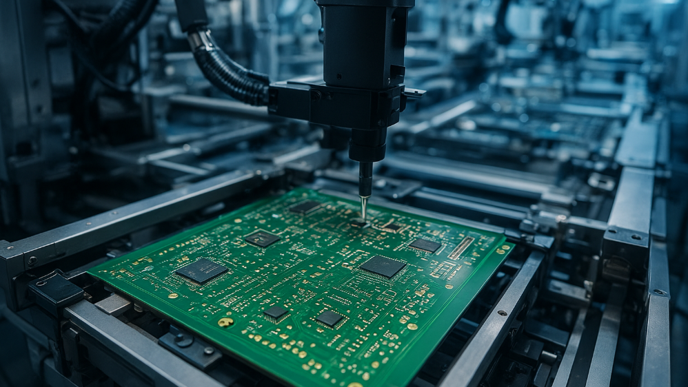
As AI computing clusters continue to expand, server interconnect architectures are undergoing major changes. High-layer-count, high-speed backplane PCBs have become critical physical platforms for rack-level interconnection. They directly influence data transmission efficiency, signal integrity, system stability, and overall computing performance.
For modern AI infrastructure, AI Server PCB manufacturing must address increasing data rates, higher interconnect density, demanding power requirements, and continuous high-load operation. This makes advanced High-Layer-Count PCB and High-Speed PCB technologies increasingly important for next-generation servers.
Manufacturing Requirements for AI Server Backplane PCBs
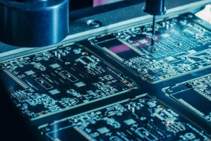
AI servers place demanding requirements on backplane construction because they must simultaneously support high-speed data transmission, power distribution, dense interconnection, and long-term reliability.
A carefully engineered multilayer structure provides sufficient routing capacity for multiple high-speed channels while maintaining stable reference planes and controlled electrical characteristics. Specialized low-loss materials can also reduce signal attenuation and help preserve signal quality across longer transmission paths.
The physical structure of a Backplane PCB is typically thicker and more complex than that of a conventional circuit board. Additional layers provide greater routing capacity and mechanical strength, while precision manufacturing ensures stable dimensional and electrical performance.
For projects requiring advanced multilayer structures, GOPCBA PCB Manufacturing supports technologies including multilayer, HDI, high-speed, high-frequency, high-TG, rigid-flex, heavy-copper, and high-layer-count PCB fabrication.
Core Manufacturing Technologies for High-Speed Backplanes
The production of a high-layer-count backplane involves multiple technically demanding processes. Material selection, stack-up design, lamination, drilling, copper plating, circuit formation, registration, inspection, and electrical testing must all work together to achieve consistent performance.
1. Precision Lamination and Layer Registration
Lamination is one of the most important stages in High-Layer-Count PCB manufacturing. Multiple copper layers and dielectric materials must be accurately bonded to form a stable multilayer structure.
Precise control of temperature, pressure, heating and cooling profiles, resin flow, and lamination time helps reduce common problems such as layer misalignment, internal voids, delamination, and board warpage.
For high-speed applications, even small variations in dielectric thickness or layer position can affect impedance and signal integrity. Therefore, accurate layer registration and repeatable lamination processes are essential.
GOPCBA’s PCB Capabilities include multilayer boards, HDI, high-TG and thick-copper PCB, high-frequency PCB, blind and buried vias, and impedance-controlled PCB technologies.
2. High-Frequency and High-Speed Material Selection
Material selection directly affects the electrical performance of an AI Server PCB. High-speed signals are sensitive to dielectric loss, dielectric thickness, copper surface characteristics, and changes in transmission-line geometry.
Depending on the design requirements, engineers may select low-loss or high-performance laminates to reduce signal attenuation and maintain predictable electrical characteristics.
Material selection should also consider thermal performance, mechanical stability, coefficient of thermal expansion, moisture resistance, and compatibility with the multilayer manufacturing process.
For high-speed designs, the PCB stack-up should be developed around the selected material system rather than treating material selection as an isolated manufacturing decision.
3. Fine-Line Routing and Precision Via Formation
AI servers require high-density interconnection because modern processors, accelerators, memory systems, and networking interfaces must exchange large volumes of data within limited board space.
Precision circuit formation enables dense routing while maintaining controlled trace geometry. Advanced via structures, including blind vias, buried vias, and microvias, can further improve routing efficiency and reduce unnecessary interconnection structures.
These technologies are particularly valuable when high-density components and high-speed interfaces must coexist within a compact multilayer architecture.
For projects involving high-density routing and advanced via structures, GOPCBA HDI PCB Design and Manufacturing Guide provides additional information about microvias, sequential buildup, stack-up development, and manufacturing considerations.
4. Controlled Impedance and Signal Integrity
High-speed backplanes require close coordination between PCB design and manufacturing. Trace width, copper thickness, dielectric thickness, dielectric constant, reference-plane position, and stack-up geometry all influence impedance.
A manufacturing process that cannot reproduce the intended physical geometry may cause impedance deviations and signal-integrity problems even when the original PCB layout has passed simulation.
Controlled-impedance manufacturing is therefore an important part of High-Speed PCB production. Engineering review, stack-up planning, impedance calculation, and manufacturing tolerance control should be considered before production begins.
GOPCBA also provides PCB Design Services covering stack-up design, impedance calculation, high-speed and high-frequency PCB design, HDI, blind and buried vias, and manufacturability optimization.
5. Manufacturing Consistency and Quality Control
High-layer-count backplanes must maintain consistent electrical and mechanical performance across production batches. Quality control therefore needs to cover the complete manufacturing process rather than relying only on final inspection.
Typical inspection and verification procedures may include automated optical inspection, dimensional inspection, X-ray inspection for complex internal structures, and electrical testing.
Process monitoring should also cover lamination, drilling, copper plating, circuit formation, surface finishing, and final inspection. This helps identify manufacturing deviations early and improves production consistency.
GOPCBA’s PCB manufacturing process includes AOI, X-ray inspection, electrical testing, process monitoring, and final quality inspection to verify circuit integrity and manufacturing consistency.
Why High-Speed Backplanes Matter for AI Servers
AI computing systems rely on rapid communication between processors, accelerators, memory, storage, and networking components. As data rates increase, the physical interconnect becomes an increasingly important part of system performance.
A properly engineered Backplane PCB can provide:
- High-density interconnection
- Stable high-speed signal transmission
- Controlled impedance
- Efficient multilayer routing
- Reliable power distribution
- Improved mechanical strength
- Consistent electrical performance
- Support for long-term high-load operation
Modern AI Server PCB designs may combine high layer counts, low-loss materials, controlled impedance, advanced via structures, and strict manufacturing tolerances to meet increasingly demanding computing requirements.
Future Development of AI Server Backplane PCBs
AI server architectures are moving toward higher computing density, faster interfaces, larger data volumes, and increasingly integrated rack-level systems. These trends will continue to raise the technical requirements for backplane PCBs.
Future High-Speed PCB solutions are expected to focus on lower transmission loss, higher signal density, more precise impedance control, improved thermal management, and increasingly sophisticated multilayer structures.
At the same time, advanced manufacturing technologies such as HDI, microvias, low-loss materials, and precision lamination will become increasingly important for supporting next-generation AI computing platforms.
GOPCBA: Advanced PCB Manufacturing for AI Computing
GOPCBA provides PCB manufacturing and assembly solutions for demanding electronic applications, including artificial intelligence, telecommunications, industrial automation, energy systems, and high-performance computing.
Our capabilities cover advanced multilayer PCB, HDI PCB, high-speed PCB, high-frequency PCB, controlled-impedance PCB, high-TG PCB, rigid-flex PCB, heavy-copper PCB, and other specialized PCB technologies.
For customers developing AI servers, data-center hardware, networking equipment, and other high-performance electronics, GOPCBA can support PCB development from engineering review and prototyping through production manufacturing and assembly.
Explore GOPCBA PCB Manufacturing Services
The combination of advanced fabrication technology, engineering support, process control, and inspection capabilities enables GOPCBA to provide reliable manufacturing solutions for increasingly complex High-Layer-Count PCB and High-Speed PCB applications.