Embedded PCB Manufacturer
Your Reliable Embedded PCB Manufacturing Partner
Modern electronic products require greater functionality in smaller spaces. Embedded PCB technology integrates selected active and passive components into the PCB structure, helping engineers reduce board size, shorten electrical interconnections, improve signal integrity, and optimize overall system performance.
A reliable Embedded PCB Manufacturer must have strong PCB fabrication capabilities, precise engineering control, advanced lamination technology, and experience with complex embedded structures. GOPCBA provides PCB manufacturing and assembly solutions for prototype, low-volume, and production requirements, supported by engineering and manufacturing capabilities across multilayer, HDI, flexible, rigid-flex, high-frequency, and other advanced PCB technologies.
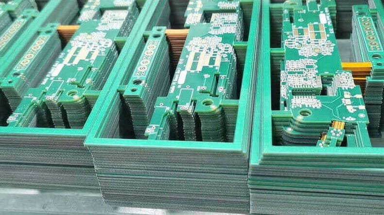
Typical embedded PCB technologies can include embedded resistors, capacitors, inductors, active components, passive components, and embedded copper structures.
Key capabilities include:
- FR-4 and high-TG PCB materials
- High-performance and high-frequency PCB materials
- Embedded resistors, capacitors, inductors, and selected active/passive components
- Multilayer PCB structures
- Blind and buried vias
- HDI and microvia technology
- Embedded copper structures for thermal management
- Engineering review and DFM support
- Electrical testing and quality inspection
For projects requiring advanced circuit structures, explore our PCB Manufacturing capabilities for additional fabrication options.
What Is an Embedded PCB?
An Embedded PCB is a printed circuit board in which selected electronic components are integrated into the internal layers or structure of the PCB rather than being mounted exclusively on the outer surface.
Embedded components can include passive devices such as resistors, capacitors, and inductors, as well as selected semiconductor or active devices. Depending on the construction method, components may be manufactured directly into the PCB or placed into precisely designed cavities within the board.
This approach can be considered an advanced form of three-dimensional PCB integration because electrical components and interconnections are distributed through different areas of the board structure.
Unlike a conventional PCB, where most components are mounted on the top or bottom surface, an Embedded Component PCB uses internal space more efficiently. This makes the technology particularly useful when board area, electrical interconnection length, thermal performance, or system size is a major design constraint.
Benefits of Embedded PCB Technology
PCB Miniaturization
Embedding components inside the PCB frees valuable surface area for other components and routing. This can help engineers create smaller electronic assemblies without sacrificing circuit functionality.
Shorter Electrical Interconnections
Embedding components closer to their electrical connections can reduce interconnection length. Shorter paths can contribute to lower parasitic effects, improved signal integrity, and better high-speed electrical performance.
Improved Signal Integrity
Reducing unnecessary interconnects can help minimize parasitic inductance and capacitance. This is particularly important for high-speed, RF, and densely routed electronic systems.
Improved Reliability
Embedded structures can reduce the number of external solder joints and connectors required by a design. Fewer interconnection points can potentially improve long-term electrical and mechanical reliability.
Better Thermal Management
Embedded copper structures can provide an efficient thermal path between heat-generating components and heat-spreading areas of the PCB. For high-power designs, PCB construction and copper distribution must be carefully engineered to control temperature rise.
More Available Surface Area
When selected components are moved inside the PCB, the external surfaces can be used more efficiently for connectors, ICs, sensors, and other components.
Compact and Cost-Optimized System Design
Although embedded PCB fabrication can involve additional manufacturing processes, integrating components can reduce board size, wiring, connectors, and assembly complexity in suitable applications.
For projects requiring compact and high-density interconnections, our HDI PCB technology provides additional options for microvias, fine-line routing, and sequential buildup structures.
THT, SMT, and Embedded Components Compared
Before selecting an embedded component technology, it is useful to understand how component integration has evolved from traditional through-hole assembly to surface-mount technology and internal PCB integration.
| Feature | Through-Hole Technology (THT) | Surface-Mount Technology (SMT) | Embedded Components |
|---|---|---|---|
| Mounting position | Component leads pass through PCB holes | Component mounted directly on surface pads | Component integrated into or placed inside PCB structure |
| Board space | Relatively large | Smaller than THT | Highly space-efficient |
| Double-sided assembly | Possible but constrained by component structure | Easily supports both sides | Surface area is supplemented by internal PCB space |
| Interconnection length | Generally longer | Shorter | Can be extremely short |
| Mechanical strength | Strong mechanical connection | High reliability when properly assembled | Integrated structure can provide excellent stability |
| Component replacement | Relatively easy | Possible with suitable rework | Difficult or impossible after final fabrication |
| Design complexity | Lower | Moderate | Higher |
| Manufacturing complexity | Conventional | Established automated process | Requires specialized PCB fabrication and engineering |
SMT remains the standard approach for many electronic products, while embedded technology is generally selected when space, electrical performance, thermal management, or system integration creates requirements beyond conventional surface assembly.
How Are Embedded PCBs Manufactured?
There are two primary approaches to producing an Embedded Component PCB.
The first approach is to manufacture passive components directly as part of the PCB structure. Embedded resistors, capacitors, and inductors can be formed using specialized materials and PCB fabrication processes.
The second approach is to place discrete components inside precisely designed cavities within the PCB stack-up. The component is then electrically connected and mechanically integrated during the PCB manufacturing process.
The appropriate approach depends on component type, electrical requirements, board thickness, material system, tolerance requirements, thermal conditions, and production volume.
Embedded PCB Manufacturing Methods
1. Embedded Component Formation
Some passive components can be fabricated directly within the PCB.
Embedded Resistor Formation
An Embedded Resistor PCB incorporates resistive material into the PCB structure rather than using a conventional surface-mounted resistor.
A resistive layer can be patterned using PCB manufacturing processes such as imaging, etching, and stripping. Specialized resistive materials, including thin-film or thick-film resistor materials, can be combined with copper structures to create the required resistance value.
The resulting resistor becomes an integrated part of the circuit rather than a separately mounted component.
Thin-film and thick-film approaches can be selected according to resistance range, accuracy, construction, and manufacturing requirements.
Embedded Inductor Formation
Embedded inductors can be formed as patterned copper structures within the PCB stack-up.
A common approach uses spiral, square, or other geometric conductor patterns distributed across one or more PCB layers. The geometry, number of turns, conductor width, spacing, and dielectric structure determine the electrical characteristics of the integrated inductor.
Compared with separately mounted inductors, embedded structures can save surface space and shorten electrical interconnections.
Embedded Capacitor Formation
An Embedded Capacitor PCB incorporates dielectric material between conductive layers to form a distributed or localized capacitance structure.
The basic construction consists of conductive electrodes separated by a dielectric layer. Depending on the technology, specialized dielectric materials with controlled electrical properties can be used to achieve the required capacitance.
The final capacitor structure becomes part of the PCB stack-up, allowing engineers to integrate capacitance into the board rather than relying entirely on discrete surface-mounted components.
2. Placement of Components Inside the PCB Core
Another method is to place discrete active or passive components inside cavities formed within the PCB.
This approach can be used for selected resistors, capacitors, inductors, and ICs.
The cavity dimensions must be carefully defined during PCB design. Component dimensions, clearance, electrical connections, mechanical tolerances, lamination pressure, and material behavior must all be considered.
Component Placement Process
The general process includes:
- Define the embedded component location during PCB design.
- Create the required cavity geometry.
- Verify component dimensions and mechanical clearance.
- Prepare the PCB layers and internal structures.
- Place the selected component into the cavity.
- Complete lamination and interconnection processes.
- Perform electrical and visual inspection.
- Conduct final testing according to project requirements.
This process requires close coordination between PCB design and manufacturing engineering.
For complex boards, our PCB Capabilities page provides additional information about advanced multilayer, HDI, high-frequency, impedance-control, and other PCB manufacturing technologies.
Embedded ICs
Embedding an IC inside a PCB requires even tighter control of cavity dimensions, component placement, interconnection, thermal management, and lamination.
The PCB designer must consider the component package, electrical connection method, thermal path, surrounding dielectric materials, and manufacturing tolerances before finalizing the design.
Because embedded ICs are inaccessible after the PCB has been fully fabricated, component quality and manufacturing inspection are particularly important.
Embedded Copper Coin PCB
Embedded copper structures are another important application of PCB embedding technology.
Copper has high thermal and electrical conductivity, making it useful for managing heat generated by high-power components.
An embedded copper coin can be incorporated into the PCB to provide a direct thermal path from a heat-generating component toward an internal copper mass or external heat-dissipation structure.
Depending on the design, thermal management can also involve thermal vias, copper planes, heat spreaders, thermal pads, or external heatsinks.
For high-current applications, our Heavy Copper PCB solutions can provide another approach to improving current-carrying capability and thermal performance.
1. Buried Copper Coin PCB
A buried copper coin is integrated inside the PCB structure so that it is not directly visible from the external surface.
Heat generated near the outer layer can be transferred through thermal vias or other conductive structures to the internal copper coin. The high thermal conductivity of copper allows heat to spread through the embedded mass and transfer toward an appropriate thermal dissipation path.
This construction can be useful for high-power components where conventional thermal vias alone may not provide sufficient thermal performance.
2. Embedded Copper Coin PCB
An embedded copper coin can also be installed into a precisely manufactured cavity after the PCB stack-up has been prepared.
The copper structure is secured within the PCB and integrated with the surrounding materials. Depending on the required thermal path, the copper coin can extend between selected PCB layers or connect directly to a component mounting area.
The exact structure should be determined according to component power, thermal resistance, board thickness, copper dimensions, and mechanical requirements.
Embedded PCB Design Considerations
Successful embedded PCB manufacturing begins with the design.
Because embedded components cannot normally be replaced after final PCB fabrication, designers should consider manufacturing feasibility from the earliest design stage.
Component Selection
Components must be compatible with the selected embedding method, PCB materials, lamination temperature, pressure, and expected operating environment.
Cavity Design
Cavity dimensions should provide sufficient clearance while maintaining the mechanical and electrical integrity of the PCB.
Thermal Management
Heat-generating embedded components require a carefully designed thermal path. Copper planes, thermal vias, embedded copper structures, and heatsinks may be combined when necessary.
Electrical Interconnection
The connection between embedded components and surrounding copper structures must satisfy current, impedance, isolation, and reliability requirements.
Stack-Up Design
The PCB stack-up must accommodate the embedded component, dielectric thickness, copper distribution, lamination requirements, and finished-board thickness.
DFM Analysis
A professional DFM review can identify problems related to component clearance, registration, cavity dimensions, copper distribution, drilling, lamination, and manufacturability before production.
Our PCB Design & Layout services can support customers during the transition from circuit design to manufacturable PCB structures.
Embedded PCB Assembly
Embedding components inside the PCB does not eliminate the need for conventional PCB assembly.
Depending on the final product, the completed board may still require SMT, THT, or mixed-technology assembly for components installed on the external surfaces.
A complete manufacturing partner can therefore support both PCB fabrication and PCBA processes.
GOPCBA provides PCB assembly services covering rigid, flexible, rigid-flex, multilayer, HDI, high-TG, high-frequency, heavy-copper, and metal-core PCB assemblies.
For projects requiring integrated fabrication and assembly, our PCB Assembly Services provide a single manufacturing path from PCB production through component assembly and inspection.
Why Choose GOPCBA for Embedded PCB Manufacturing?
Advanced Manufacturing Experience
Embedded PCB manufacturing requires more than standard circuit-board fabrication. It involves material selection, stack-up engineering, cavity design, component integration, lamination control, and inspection.
GOPCBA provides PCB fabrication and PCBA manufacturing capabilities for complex electronic products, supported by engineering services including DFM/DFA analysis, Gerber review, stack-up evaluation, and manufacturing feasibility assessment.
Flexible Design and Manufacturing Support
Every embedded PCB project has different electrical, mechanical, thermal, and manufacturing requirements.
Our engineering approach can support different PCB constructions, including multilayer, HDI, high-frequency, high-TG, flexible, rigid-flex, heavy-copper, and controlled-impedance designs.
Quality Control and Testing
Complex PCB structures require reliable inspection throughout the manufacturing process.
Depending on the product requirements, PCB manufacturing and assembly can include automated optical inspection, electrical testing, X-ray inspection, and other quality-control processes.
Prototype to Production
Embedded PCB technology is often introduced during product development when conventional PCB construction can no longer meet size, performance, or integration requirements.
A manufacturing partner capable of supporting both prototypes and production can help reduce transition risks and maintain consistency as the project moves toward volume manufacturing.
One-Stop PCB and PCBA Manufacturing
GOPCBA provides an integrated manufacturing model covering PCB fabrication, component sourcing, PCB assembly, testing, and related electronic manufacturing services.
This integrated approach can simplify supplier management and help engineering teams coordinate PCB fabrication and assembly requirements through one manufacturing partner.
Get an Embedded PCB Quote
An Embedded PCB can provide significant advantages when conventional surface-mounted components cannot meet the required size, electrical, thermal, or integration requirements.
However, embedded technology requires careful consideration of PCB materials, component selection, cavity design, stack-up, lamination, thermal management, electrical interconnections, and manufacturing tolerances.
GOPCBA supports advanced PCB manufacturing and assembly requirements from prototype development through production. If you are developing an embedded resistor PCB, embedded capacitor PCB, embedded inductor structure, embedded IC design, or embedded copper thermal solution, provide your Gerber files, stack-up information, BOM, drawings, and technical requirements for engineering evaluation.
Contact GOPCBA to discuss your embedded PCB manufacturing requirements and request a quotation.
Frequently Asked Questions
What is an embedded component PCB?
An embedded component PCB is a circuit board that integrates selected electronic components into the internal layers or structure of the PCB rather than mounting all components on the external surface.
What components can be embedded in a PCB?
Depending on the manufacturing technology, resistors, capacitors, inductors, and selected active components such as ICs can be embedded. Copper structures can also be integrated for thermal management.
What are the main advantages of embedded PCBs?
The main advantages include reduced board size, shorter electrical interconnections, improved space utilization, potentially improved signal integrity, enhanced integration, and additional thermal-management options.
Are embedded PCBs more expensive than conventional PCBs?
Embedded PCB manufacturing can be more expensive because it may require specialized materials, cavity formation, additional process steps, tighter engineering controls, and more complex inspection. However, the total system cost can potentially be reduced when embedding eliminates connectors, wiring, board area, or additional components.
Can embedded PCBs use SMT and THT components?
Yes. Embedded components can coexist with conventional surface-mounted and through-hole components. The external portions of the finished PCB can still undergo SMT, THT, or mixed-technology assembly.
Can embedded PCBs be used for high-speed applications?
Yes. Embedded structures can be useful in high-speed designs because shorter interconnections may help reduce parasitic effects. However, signal integrity depends on the complete stack-up, material system, impedance structure, routing, and manufacturing tolerances.
Can embedded copper be used for thermal management?
Yes. Embedded copper coins and other internal copper structures can provide efficient thermal paths for high-power components. The appropriate structure depends on the component’s power dissipation and overall thermal design.
What information is needed for an embedded PCB quotation?
A typical engineering package should include Gerber or ODB++ files, PCB stack-up, mechanical drawings, BOM, component specifications, embedded-component locations, material requirements, copper thickness, surface finish, quantity, and applicable electrical or reliability requirements.
Is embedded PCB technology suitable for mass production?
It can be suitable for production when the design has been validated and the manufacturing process is properly controlled. Early DFM analysis and prototype verification are recommended before moving into volume production.
Start Your Embedded PCB Project
Whether you need an Embedded PCB Manufacturer for a compact electronic device, high-density circuit, high-speed application, power-management system, or thermally demanding product, successful results depend on close coordination between PCB design, materials, fabrication, component integration, and assembly.
GOPCBA provides advanced PCB manufacturing and assembly capabilities to help customers move from engineering development to reliable production.
Request a quotation today and let our engineering team evaluate your embedded PCB requirements.