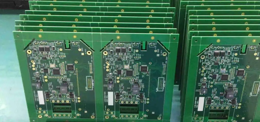
Free PCB File Check and DFM Analysis
A successful PCB project starts with a manufacturable design. Even when a PCB design appears electrically correct, problems in materials, stack-up, drilling, copper spacing, solder mask, BGA routing, impedance, or panelization can create manufacturing difficulties, assembly defects, increased costs, or unexpected delays.
A professional PCB File Check helps identify potential manufacturing risks before production begins. During a comprehensive PCB DFM Analysis, engineers review Gerber files, drill files, drawings, stack-up information, and other manufacturing documentation to determine whether the design is suitable for reliable production.
For complex boards, early PCB Design Review is especially important. Issues identified before fabrication are generally much easier and less expensive to correct than defects discovered after PCB production or assembly.
GOPCBA provides engineering-focused PCB manufacturing support from prototype development through production. Its manufacturing services cover conventional multilayer boards as well as HDI, high-frequency, high-TG, heavy-copper, flexible, and rigid-flex technologies.
Why Is DFM Important for PCB Manufacturing?
DFM, or Design for Manufacturing, is the process of evaluating a PCB design against actual manufacturing capabilities and process limitations.
A good PCB DFM Analysis can identify problems that may not be obvious during schematic capture or PCB layout.
Typical reasons for performing DFM include:
- Design errors introduced during PCB development
- Data conversion errors between different CAD formats
- Manufacturing processes or materials that are not compatible with the selected design
- Insufficient copper spacing or annular ring dimensions
- Improper via or drill structures
- Solder mask openings that are difficult to manufacture
- BGA routing and soldering risks
- Inadequate stack-up or dielectric thickness
- Impedance-control problems
- Panelization issues
- Unnecessary manufacturing costs
Early DFM evaluation can also identify opportunities to optimize materials, stack-up structures, panel utilization, and manufacturing processes.
For projects requiring professional engineering support, GOPCBA also provides PCB Design and Layout Services, including DFM evaluation, impedance calculation, stack-up design, EMC inspection, and manufacturing optimization.
What Does a Professional PCB File Check Include?
During a comprehensive PCB Design Review, engineers should evaluate the complete manufacturing data rather than checking only the Gerber files.
Typical review items include:
- Gerber files
- NC drill files
- PCB drawings
- Stack-up information
- Material specifications
- Copper thickness
- Solder mask files
- Silkscreen files
- Component and BGA information
- Impedance requirements
- Special manufacturing instructions
- Panelization requirements
- Netlist information
The purpose is to ensure that the customer’s design intent is preserved while making the board practical for manufacturing.
Material Selection and Stack-Up Review
Material selection has a direct impact on PCB reliability, electrical performance, thermal behavior, and manufacturing cost.
Sometimes a specified material may have an unusually long lead time, limited availability, or may not be suitable for a particular manufacturing process. In such cases, an appropriate alternative material may be proposed for engineering approval.
Material selection should consider:
- PCB thickness
- Copper thickness
- Dielectric thickness
- Tg requirements
- Electrical characteristics
- Thermal requirements
- High-frequency performance
- Mechanical reliability
- Availability and lead time
For high-speed and RF applications, material selection becomes even more important because dielectric constant and dissipation factor can directly influence signal integrity and impedance.
GOPCBA’s PCB Manufacturing Services support materials including standard FR-4, high-TG materials, Rogers, aluminum, flexible materials, and rigid-flex constructions.
PCB Panel Utilization
Panelization can also influence manufacturing cost.
For high-volume production, an appropriate array design can improve material utilization and reduce waste. Engineers may evaluate different panel arrangements to achieve a practical balance between:
- PCB utilization
- Production efficiency
- Routing requirements
- Assembly handling
- Depanelization
- Manufacturing cost
Panelization should therefore be considered during the engineering stage rather than after PCB fabrication has already been planned.
Drill Design and Tolerance Review
Drilling is one of the most important parts of a PCB manufacturing process.
A professional PCB File Check should verify hole sizes, tolerances, drill types, annular rings, hole-to-copper clearances, and special drilling requirements.
Hole Tolerances
Engineers should verify whether the specified hole dimensions and tolerances are realistic for the selected manufacturing process.
Special holes, including press-fit holes, may require tighter dimensional control to ensure reliable assembly.
For press-fit applications, hole tolerance should be carefully controlled according to the component manufacturer’s requirements.
Via Design
Vias that are too small may create difficulties during drilling, plating, cleaning, and solder-mask processing.
Common DFM considerations include:
- Via diameter
- Finished hole size
- Pad size
- Annular ring
- Via-to-pad spacing
- Via-to-trace spacing
- Solder-mask coverage
- Via plugging
- Resin filling
- Via-in-pad requirements
Vias located close to BGA pads may require special treatment to prevent solder from entering the hole during assembly.
In high-density applications, filled and capped vias or via-in-pad structures may be considered to improve routing density and assembly reliability.
GOPCBA’s published PCB Capabilities include HDI, blind and buried vias, impedance-controlled boards, high-frequency PCBs, heavy-copper PCBs, and other advanced PCB structures.
Blind and Buried Vias
Blind and buried vias are commonly used to increase routing density in multilayer and HDI PCBs.
The selected via structure should be compatible with:
- Layer stack-up
- Dielectric thickness
- Laser-drilling capability
- Mechanical drilling
- Copper plating
- Sequential lamination
- Aspect ratio
- Reliability requirements
An optimized stack-up can sometimes reduce manufacturing complexity while still achieving the required routing density.
Back Drilling and Depth-Controlled Features
Back Drilling
Back drilling removes the unused portion of a plated through-hole via.
The purpose is to reduce the electrical stub length and minimize unwanted signal effects such as:
- Signal reflection
- Scattering
- Insertion loss
- Delay
- Impedance discontinuity
Back drilling is particularly useful for high-speed digital and high-frequency applications.
Typical engineering parameters include:
| Parameter | Typical Reference |
|---|---|
| Back-drill diameter | PTH diameter + 0.15 mm |
| Back-drill depth tolerance | ±0.05 mm |
| Minimum remaining stub | 0.05 mm |
Actual values should always be confirmed against the manufacturer’s current process capability.
Depth-Controlled Routing
Depth-controlled routing can be used when a specific cavity, controlled-depth feature, or mechanical structure is required.
The design should define the required depth, tolerance, remaining material thickness, and relationship to internal copper layers.
Copper Plating and Copper Distribution
Uniform copper distribution is essential for stable PCB manufacturing.
Uneven copper density can influence:
- Plating thickness
- Etching
- Line width
- Board deformation
- Electrical performance
- Manufacturing yield
Copper balancing features may be added to appropriate areas of a panel to improve plating uniformity.
After plating, actual copper thickness should be verified against the specified requirements.
For advanced projects, GOPCBA provides a broad range of manufacturing capabilities, including controlled-impedance, high-frequency, heavy-copper, HDI, and multilayer PCB technologies.
Lamination and Stack-Up Optimization
The lamination structure must be compatible with the required board thickness, dielectric thickness, copper weight, via structure, and electrical specifications.
An unsuitable stack-up can cause:
- Delamination
- Insufficient dielectric thickness
- Electrical breakdown
- Impedance deviation
- Excessive resin flow
- Reliability problems
- Difficulty manufacturing blind vias
For boards with blind vias or HDI structures, material selection and sequential lamination must be evaluated together.
Dielectric Thickness
The dielectric layer should be thick enough to satisfy electrical isolation, impedance, and mechanical requirements.
For multilayer PCBs, engineering should verify the actual dielectric thickness between copper layers before production.
Quality inspection should also confirm the finished dielectric structure against the approved stack-up.
CAM Data and Engineering Analysis
CAM engineering is responsible for converting customer manufacturing data into production-ready files.
A professional CAM process should include:
- Data import
- Gerber verification
- Drill-file verification
- DFM analysis
- Copper compensation
- Solder-mask optimization
- Silkscreen optimization
- Panelization
- Netlist verification
- Final production-data output
All customer-supplied files should be compared with the final production data to ensure that no unintended changes have been introduced.
BGA Design and Routing Review
BGA components require special attention because their pitch, pad size, via structure, and routing density can directly affect PCB manufacturability and assembly yield.
BGA Solder Mask
A typical engineering reference is:
BGA solder-mask opening = BGA pad size + approximately 4 mil
However, the final solder-mask design should be determined according to BGA pitch, pad size, PCB fabrication capability, solder-mask registration, and assembly requirements.
For very small BGA pads, solder-mask-defined pads may be considered when conventional non-solder-mask-defined pads cannot provide sufficient manufacturing control.
BGA Layout Recommendations
To improve BGA routing and assembly reliability:
- Avoid placing unnecessary components immediately around the BGA.
- Maintain adequate routing space around the package.
- Route traces consistently between BGA pads.
- Keep differential pairs symmetrical and properly coupled.
- Avoid unnecessary routing detours.
- Optimize power and ground connections.
- Use appropriate via structures.
- Consider via plugging or filling where required.
- Keep solder-mask design within the manufacturer’s process capability.
For complex BGA and high-density projects, an early PCB Design Review can help identify routing, impedance, stack-up, and manufacturing risks before fabrication.
Controlled Impedance Simulation
Controlled impedance is essential for many high-speed and RF PCB designs.
An impedance analysis should consider:
- Trace width
- Copper thickness
- Dielectric thickness
- Dielectric constant
- Reference-plane location
- Differential-pair spacing
- Surface finish
- Stack-up structure
Common controlled-impedance requirements include 50-ohm single-ended and 90-ohm or 100-ohm differential structures, depending on the interface and design specification.
The calculated impedance should be reviewed before manufacturing.
For high-speed and high-frequency boards, PCB fabrication capability must match the design requirements. GOPCBA supports controlled-impedance, high-frequency, and high-speed PCB manufacturing technologies.
Panelization and V-Score Design
Many customers provide individual PCB designs, but panelization can improve both PCB fabrication and PCB assembly efficiency.
Two common methods are:
- V-score
- Tab routing or mouse-bite routing
V-Score Design Guidelines
Typical engineering considerations include:
- For a 30° V-score, copper should generally be more than 0.35 mm from the V-score centerline.
- For a 45° V-score, copper should generally be more than 0.40 mm from the V-score centerline.
- Thin boards may require single-sided V-scoring.
- Boards above approximately 1.0 mm may require an appropriate remaining thickness.
- Boards above 1.6 mm generally require a larger residual thickness.
- Sharp board edges should be avoided where possible.
The exact values should be confirmed with the PCB manufacturer’s current fabrication rules.
Copper Trace and Spacing Rules
Copper design must account for manufacturing compensation and etching capability.
A professional PCB Design Rules review should verify:
- Minimum trace width
- Minimum spacing
- Copper-to-hole clearance
- Copper-to-board-edge clearance
- Pad dimensions
- Annular rings
- Copper-to-solder-mask spacing
- Copper density
- Etching compensation
If a design does not meet the manufacturing minimum, engineers may optimize selected features where doing so does not change the customer’s electrical requirements.
However, controlled-impedance traces and other critical electrical features should not be moved or resized without customer approval.
IC Pin and Trace Optimization
When a trace connected to an IC pin is wider than the pin itself, the trace may need to be narrowed locally to maintain adequate spacing.
The transition should be kept as short as practical and should not compromise electrical performance.
Copper Near the PCB Edge
Copper and traces should maintain sufficient clearance from the finished board outline.
This is particularly important when routing near:
- Routed edges
- V-score lines
- Plated slots
- Mechanical holes
- Depanelization areas
Adequate edge clearance helps prevent exposed copper and mechanical damage after routing or depanelization.
Solder Mask Design
Solder mask design is critical for PCB fabrication and assembly.
A PCB DFM Analysis should review the solder-mask Gerber files to identify:
- Missing solder-mask openings
- Excessively small solder-mask dams
- Incorrect pad openings
- Unwanted mask coverage
- BGA solder-mask problems
- PTH and NPTH mask issues
- Via tenting requirements
General Solder-Mask Guidelines
The solder-mask opening is normally designed slightly larger than the copper pad to compensate for registration tolerances.
The required expansion depends on:
- Copper thickness
- Pad geometry
- PCB layer
- Solder-mask process
- Board density
- Fabricator capability
As copper thickness increases, solder-mask registration and opening requirements may change.
For BGA applications, solder-mask openings should be designed according to the actual BGA pitch and fabrication capability rather than using a universal value.
PTH Solder-Mask Design
For plated through-holes, the solder-mask opening should be reviewed to ensure that the required hole and pad areas remain properly exposed.
Special attention should be given to small holes where excessive solder-mask coverage may interfere with assembly.
NPTH Solder-Mask Design
For non-plated through-holes, the solder-mask opening depends on the hole diameter and mechanical requirements.
A typical engineering approach is to use different mask expansions for smaller and larger NPTH holes.
The final dimensions should be verified according to the fabricator’s current process capability.
Carbon Ink Design
Carbon ink is commonly used for:
- Keypads
- Contact pads
- Membrane switches
- Conductive buttons
- Wear-resistant contact surfaces
Typical design references include:
- Printed carbon pad larger than the copper pad by at least 10 mil
- Minimum carbon line width: 10 mil
- Minimum carbon pad-to-pad spacing: 10 mil
- Adequate clearance from plated holes and other copper features
Carbon ink should not overlap unintended pads, holes, or conductive areas.
Silkscreen Design
Silkscreen must remain readable after PCB fabrication and assembly.
Typical design considerations include:
- Minimum line width
- Minimum character height
- Character spacing
- Pad clearance
- Polarity markings
- Component reference designators
- Orientation indicators
- UL markings
- Date codes
As a practical reference:
- Minimum silkscreen line width: approximately 5–6 mil
- Minimum character height: approximately 0.8 mm
- Minimum character-to-character spacing: approximately 6 mil
- Minimum character-to-pad clearance: approximately 6 mil
Silkscreen should not cover solderable pads unless specifically required.
Incorrectly mirrored bottom-side text should also be corrected before manufacturing.
Netlist Verification
Netlist verification is an important part of the engineering review process.
The production data should be compared against the original design netlist to identify unintended changes that could result in:
- Open circuits
- Short circuits
- Incorrect connections
- Missing connections
- Manufacturing-data errors
For high-density and complex PCBs, netlist verification provides an additional layer of protection against production errors.
Internal Pad and Annular Ring Optimization
Internal pads must have sufficient connection area to maintain reliable electrical and mechanical connections.
Typical annular-ring requirements depend on:
- Finished hole size
- Drill size
- Copper thickness
- Layer type
- Manufacturing tolerance
Engineering compensation may be applied when the designed annular ring is insufficient for the selected fabrication process.
Typical Inner Annular Ring References
| Copper Weight | Typical Additional Copper per Side |
|---|---|
| 1 oz | ≥0.10 mm |
| 2 oz | ≥0.13 mm |
| 3 oz | ≥0.20 mm |
| 4 oz | ≥0.30 mm |
These values are engineering references and should be validated against the manufacturer’s current process specifications.
Teardrop Design
Teardrops can improve the connection between pads and traces, especially when a relatively narrow trace connects to a drilled pad.
They can help improve:
- Drill registration tolerance
- Mechanical reliability
- PTH connection strength
- Manufacturing yield
Teardrops should be added only when adequate spacing remains available.
Internal Functional Pads
Internal functional pads should maintain sufficient clearance from surrounding copper features.
Where appropriate, an internal isolation ring may be maintained around the pad.
Typical minimum clearances depend on the board’s manufacturing process and minimum spacing capability.
Removing Non-Functional Features
Non-functional internal pads may sometimes be removed to reduce manufacturing risk and unnecessary copper structures.
Exceptions may apply to:
- Blind vias
- Buried vias
- HDI structures
- Customer-specific requirements
Removing unnecessary internal features can help reduce the possibility of unintended internal shorts and improve manufacturing consistency.
Additional PCB Manufacturing Optimization
Other optimization opportunities may include:
- Copper balancing
- Resin-flow optimization
- Rounded internal copper corners
- Improved panel utilization
- Via plugging
- Via filling
- Solder-mask optimization
- Silkscreen cleanup
- Netlist verification
- Stack-up optimization
- Impedance verification
For projects requiring both PCB fabrication and assembly, integrating engineering review with manufacturing can reduce communication gaps and improve production consistency.
GOPCBA offers integrated PCB Assembly Services covering rigid, flexible, rigid-flex, multilayer, HDI, heavy-copper, metal-core, high-TG, high-frequency, and controlled-impedance PCB assemblies.
DFM Review Before PCB Production
A comprehensive PCB DFM Analysis should ideally be completed before the final manufacturing data is released.
A typical workflow includes:
- Receive Gerber and manufacturing files
- Verify file completeness
- Check PCB materials and stack-up
- Review drill data
- Check vias and annular rings
- Review copper spacing
- Verify solder-mask design
- Review BGA structures
- Simulate controlled impedance
- Check panelization
- Verify silkscreen
- Run netlist comparison
- Optimize manufacturing data
- Confirm special requirements
- Release final CAM data
This approach helps identify manufacturing problems while they are still easy to correct.
From PCB Design Review to PCB Assembly
A PCB should not be evaluated only from a fabrication perspective. Assembly requirements should also be considered before production.
BGA, fine-pitch components, small passive components, solder-mask design, fiducials, panelization, component spacing, and test requirements can all affect assembly yield.
For customers requiring prototype or small production quantities, GOPCBA also provides Low Volume PCB Assembly, including SMT and DIP assembly, multiple PCB types, engineering support, and DFM review.
For more complex manufacturing programs, GOPCBA’s PCBA Capabilities cover turnkey, partial-turnkey, and kitted assembly, as well as SMT and through-hole processes.
Why Choose Professional PCB Engineering Support?
Professional engineering review can help reduce the risk of manufacturing problems before they become expensive production issues.
The main benefits include:
- Earlier identification of design problems
- Improved manufacturing yield
- Reduced PCB fabrication risk
- Better assembly compatibility
- More predictable production costs
- Improved material selection
- Optimized stack-up
- Better signal-integrity performance
- Reduced redesign requirements
- Faster transition from prototype to production
For flexible and rigid-flex applications, manufacturing rules are even more important because mechanical bending, copper thickness, material selection, and assembly processes must be considered together. GOPCBA also provides Flex and Rigid-Flex PCB Assembly for applications requiring compact, lightweight, and flexible circuit structures.
Start Your PCB File Check
A reliable PCB manufacturing process begins with reliable engineering data.
Before releasing your next PCB project for production, review the complete design for material compatibility, drill tolerances, via structures, copper spacing, stack-up, impedance, BGA routing, solder mask, silkscreen, panelization, and assembly requirements.
A professional PCB File Check and PCB Design Review can identify potential manufacturing problems before fabrication starts, helping improve yield, control costs, and accelerate the transition from prototype to production.
If you are ready to discuss a new PCB project, prototype, or production order, visit GOPCBA Contact Us to submit your PCB files and project requirements.