Layered Rigid-Flex PCB
Modern electronic products increasingly require circuit boards that combine high circuit density, mechanical strength, compact packaging, and three-dimensional flexibility. A layered rigid-flex PCB integrates rigid circuit sections with flexible circuit sections in a multilayer structure, providing both the structural stability of a rigid board and the bending capability of a flexible circuit.
This technology is particularly useful when electronic assemblies must fit into limited spaces, follow irregular mechanical contours, withstand vibration, or reduce the number of cables and connectors.
GOPCBA provides PCB fabrication and assembly solutions for rigid, flexible, and rigid-flex circuit technologies. Its manufacturing capabilities cover complex multilayer structures, HDI, controlled impedance, blind and buried vias, and other advanced PCB technologies. PCB Manufacturing Services
What Is a Rigid-Flex PCB?
A rigid-flex PCB combines rigid PCB sections and flexible circuit sections into one integrated printed circuit board. The rigid sections provide mechanical support for components and connectors, while the flexible sections allow the circuit to bend, fold, or conform to the shape of an enclosure.
Flexible sections are commonly constructed with polyimide-based materials and copper conductors, while rigid sections can use FR-4 or other high-performance PCB laminates.
Unlike a system consisting of separate rigid boards connected by cables, a rigid-flex construction integrates the electrical interconnection directly into the PCB structure. This can reduce connection points, simplify assembly, save space, and improve overall reliability.
For applications requiring both flexibility and structural support, the combination of flexible PCB technology and rigid PCB construction provides significant design freedom.
What Is a Layered Rigid-Flex PCB?

A layered rigid-flex PCB is a rigid-flex circuit containing multiple conductive and dielectric layers within its rigid and flexible regions. Each layer can be assigned a specific electrical or mechanical function, such as signal routing, power distribution, grounding, shielding, or structural support.
Depending on the product requirements, a multilayer rigid-flex structure may contain several rigid layers combined with one or more flexible layers. The layer configuration is determined by circuit density, impedance requirements, mechanical movement, component placement, thermal conditions, and available installation space.
A properly engineered multilayer rigid-flex PCB can therefore provide much greater routing density than a simple single-layer flexible circuit while maintaining controlled flexibility in designated bending areas.
For advanced PCB fabrication, GOPCBA supports multilayer boards and complex structures from prototype through production. GOPCBA PCB Fabrication Capabilities
Key Features of Layered Rigid-Flex PCBs
A layered rigid-flex design has several important characteristics that distinguish it from conventional rigid or flexible PCBs.
Multilayer Circuit Architecture
Multiple conductive layers can be arranged within the rigid sections to accommodate high-density signal routing, power distribution, and grounding requirements. The flexible region is designed with an appropriate number of copper layers to maintain the required bending performance.
Dedicated Flexible Regions
The flexible portion is normally positioned between rigid sections and acts as an integrated electrical interconnect. This allows different rigid circuit areas to move relative to one another without requiring separate cables.
Controlled Layer Stack-Up
The layer stack-up must be carefully engineered to maintain electrical performance and mechanical reliability. Signal, power, and ground layers need to be positioned appropriately to control impedance, reduce electromagnetic interference, and provide predictable return-current paths.
Component Placement
Components can be mounted on rigid areas in conventional configurations. Components may also be mounted on designated flexible regions when the stack-up, coverlay, pad structure, bend requirements, and assembly process are specifically designed for this purpose.
Reinforcement and Bend Control
Stiffeners can be added to selected areas where additional mechanical support is required. Bend zones must be clearly defined so that components, vias, copper features, and other rigid structures are not subjected to excessive mechanical stress.
Why Use Layered Rigid-Flex PCBs?
The adoption of a layered rigid-flex structure can provide significant advantages for compact and mechanically demanding electronic products.
Higher Circuit Density
Additional layers provide more routing space for complex circuits. Designers can accommodate high pin-count devices, power networks, high-speed signals, and grounding structures without increasing the overall board footprint excessively.
Space and Weight Reduction
A rigid-flex structure can replace multiple rigid PCBs, wire harnesses, and connectors with a single integrated circuit assembly.
This can reduce overall package size and weight, making the technology especially attractive for portable electronics, aerospace equipment, medical devices, and automotive systems.
Three-Dimensional Design Freedom
Conventional rigid PCBs are primarily designed for planar installation. A rigid-flex structure can be folded or routed through three-dimensional mechanical spaces.
This makes it possible to design electronics around curved housings, compact enclosures, moving mechanisms, and irregular internal structures.
Fewer Connectors and Cables
Connectors and cable assemblies introduce additional components and potential failure points. By integrating electrical connections directly into the PCB, rigid-flex technology can reduce the number of interconnection points.
This can simplify assembly and improve long-term system reliability.
Improved Mechanical Reliability
When correctly designed, flexible interconnects can tolerate repeated movement and vibration better than conventional cable connections. The integrated structure also reduces the number of detachable electrical interfaces.
Simplified Assembly
A single integrated PCB can replace multiple boards and cable assemblies. This can reduce assembly operations, improve manufacturing consistency, and simplify the overall product architecture.
For customers requiring complete manufacturing from bare PCB fabrication through assembly, GOPCBA also provides PCB assembly capabilities for rigid, flexible, and rigid-flex boards. PCB Assembly Services
Layered Rigid-Flex PCB Manufacturing Process
Manufacturing a layered rigid-flex circuit requires precise control of materials, layer alignment, lamination, drilling, plating, coverlay application, and electrical testing.
Material Selection
Material selection directly affects electrical performance, flexibility, thermal resistance, dimensional stability, and product lifetime.
Polyimide is widely used for flexible sections because it offers good electrical and mechanical performance. FR-4 and high-Tg laminates can be used for rigid sections where greater structural strength and thermal performance are required.
Depending on the application, manufacturers may also use high-performance dielectric materials, low-loss laminates, adhesive systems, and specialized copper foils.
The material system should be selected according to operating temperature, bend cycles, signal frequency, impedance requirements, and environmental conditions.
Material Preparation
Before lamination, copper-clad laminates, flexible materials, cores, prepregs, adhesive films, and other materials must be prepared and cleaned.
Surface cleanliness is important because contamination can negatively affect adhesion, copper bonding, and subsequent manufacturing processes.
Layer Alignment and Lamination
The individual layers are accurately registered and stacked according to the engineering-approved stack-up.
Controlled heat, pressure, and vacuum conditions are then applied during lamination to bond the layers together.
Rigid and flexible areas require different mechanical considerations, so the lamination process must account for the thickness, material characteristics, and dimensional behavior of each region.
Circuit Imaging
A photoresist or dry-film material is applied to the copper surface. The desired circuit pattern is transferred through imaging technology.
After development, the exposed copper areas can be processed to create the required conductor pattern.
Etching
Unwanted copper is removed through a controlled chemical etching process. The remaining copper forms the required signal traces, pads, power structures, and ground connections.
For high-density designs, accurate etching control is especially important because excessive undercutting can affect trace width and impedance.
Mechanical and Laser Drilling
Drilling creates vias, through-holes, mounting holes, and other required openings.
Depending on the stack-up, mechanical drilling and laser drilling may both be used. Laser drilling is particularly useful for microvias and high-density interconnection structures.
Copper Plating
Copper is deposited inside drilled holes and on selected PCB surfaces to establish electrical connections between layers.
Reliable plating is essential because via structures must withstand electrical current, thermal cycling, and mechanical stresses throughout the product’s operating life.
Coverlay Application
Flexible areas commonly use a polyimide coverlay to protect copper conductors and provide electrical insulation.
The coverlay opening pattern must be accurately aligned with component pads, contact areas, vias, and other exposed copper features.
Stiffener Application
Local stiffeners may be added to connector areas, component mounting areas, or other regions requiring additional mechanical support.
Stiffeners should only be used where necessary because excessive reinforcement can restrict the intended flexibility of the circuit.
Surface Finishing
Exposed copper surfaces can receive finishes such as ENIG, immersion silver, immersion tin, HASL, OSP, ENEPIG, or gold plating depending on the application and assembly requirements.
The selected finish affects solderability, contact performance, corrosion resistance, and long-term reliability.
PCB Separation and Routing
After fabrication and finishing, the individual circuits are separated from the production panel using appropriate routing, punching, laser cutting, or other controlled methods.
The separation process must avoid excessive mechanical stress on flexible sections and transition zones.
Electrical Testing and Inspection
Final inspection verifies dimensional accuracy, conductor integrity, hole quality, surface finish, and other manufacturing requirements.
Electrical testing can identify open circuits and short circuits before shipment. Depending on production requirements, flying probe testing, fixture testing, AOI, X-ray inspection, impedance testing, and other inspection methods can also be incorporated.
GOPCBA supports PCB prototyping and production with engineering review, DFM analysis, manufacturing, inspection, and testing services. Rapid PCBA Prototyping
Common Layer Configurations
Layered rigid-flex PCB structures can be customized according to the electrical and mechanical requirements of the final product.
Typical configurations include:
- 2 rigid layers with 1 flexible layer
- 3 rigid layers with 1 flexible layer
- 4 rigid layers with 2 flexible layers
- 4 rigid layers with 2 flexible layers and a ZIF interface
- 5 rigid layers with 3 flexible layers
- 6 rigid layers with 4 flexible layers
The actual configuration should not be selected solely according to the number of layers. Designers should consider bend radius, copper distribution, dielectric thickness, impedance, component placement, thermal performance, and manufacturability.
Important Design Considerations
Control the Bend Area
The flexible bend region should be clearly separated from rigid areas and component mounting zones.
Components, solder joints, large vias, and other mechanically rigid structures should generally be kept away from areas subjected to repeated bending unless the design has been specifically engineered for dynamic flexing.
Optimize Copper Distribution
Uneven copper distribution can contribute to dimensional instability and mechanical stress.
Copper patterns should therefore be balanced wherever practical, particularly around rigid-to-flex transition zones.
Plan Signal and Ground Layers Carefully
High-speed and sensitive signals require appropriate reference planes and return-current paths.
Ground layers should be arranged to reduce electromagnetic interference and minimize unwanted coupling between signal groups.
Separate Sensitive Analog and Digital Circuits
When a product contains both analog and digital circuitry, the layout should be carefully partitioned according to system requirements.
Signal routing, grounding, power distribution, and return paths should be analyzed as part of the overall electrical design rather than treating each layer independently.
Consider Thermal Management
Increasing the number of layers does not automatically guarantee better thermal performance. Designers should evaluate copper distribution, heat-generating components, thermal vias, component placement, and the mechanical enclosure together.
For demanding applications, thermal simulation and DFM review can help identify potential manufacturing and reliability problems before production.
Layered Rigid-Flex PCB Applications
Consumer Electronics
Smartphones, laptops, tablets, wearable devices, cameras, and other compact electronic products can benefit from rigid-flex construction.
The flexible sections allow circuits to follow compact mechanical structures while the rigid areas provide stable platforms for processors, connectors, sensors, and other components.
Medical Electronics
Medical devices often require compact electronics with high reliability and controlled mechanical movement.
Rigid-flex technology can be used in portable medical equipment, diagnostic systems, imaging equipment, wearable medical electronics, and other products where space and reliability are important.
Automotive Electronics
Automotive electronics must withstand vibration, temperature changes, mechanical movement, and long operating periods.
Applications can include vehicle control systems, navigation electronics, sensor modules, instrument systems, and other distributed electronic assemblies.
GOPCBA also provides PCB solutions for automotive electronics and supports applications requiring rigid, flexible, and rigid-flex circuit technologies. Automotive PCB Solutions
Aerospace and Defense
Aerospace and defense electronics often face strict requirements for weight, space utilization, vibration resistance, reliability, and environmental performance.
Rigid-flex circuits can reduce wiring and connector count while allowing electronic assemblies to conform to complex mechanical structures.
Industrial Equipment
Industrial control equipment, robotics, instrumentation, automation systems, and sensing equipment can use rigid-flex circuits where conventional wiring is difficult to install.
The ability to integrate multiple circuit sections into a single assembly can simplify system architecture and improve installation efficiency.
For industrial applications, PCB requirements may vary substantially according to operating environment, production volume, electrical design, and mechanical constraints. GOPCBA offers dedicated industrial PCB assembly solutions for customized applications. Industrial PCB Assembly
Layered Rigid-Flex PCB vs. Conventional PCB
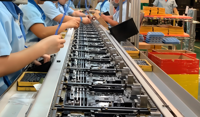
The primary difference is the ability to combine structural rigidity with controlled flexibility.
A conventional rigid PCB is well suited to flat installations where the circuit does not need to move. A flexible PCB provides excellent bendability but may require additional mechanical support for certain components.
A layered rigid-flex PCB combines the two approaches. Rigid areas can support components and connectors, while flexible areas provide electrical connections through three-dimensional mechanical paths.
This makes rigid-flex particularly valuable when reducing cables, connectors, assembly space, and overall system complexity is more important than minimizing the initial PCB fabrication cost.
How to Choose a Layered Rigid-Flex PCB Manufacturer
When selecting a manufacturing partner, engineers should evaluate more than the manufacturer’s basic layer count.
Important criteria include:
- Rigid and flexible PCB manufacturing experience
- Multilayer fabrication capability
- Material selection and supply chain
- Flexible-region manufacturing expertise
- Layer alignment and registration control
- Mechanical and laser drilling capability
- Copper plating quality
- Controlled impedance capability
- DFM and engineering support
- Electrical testing and inspection
- Prototype and production capacity
- PCB assembly capabilities
A manufacturer capable of handling both PCB fabrication and assembly can also reduce communication between multiple suppliers and simplify project management.
GOPCBA offers integrated PCB manufacturing, component sourcing, SMT, DIP, testing, and finished-product assembly services, allowing customers to manage multiple stages through one manufacturing partner. One-Stop PCB Assembly Solutions
Conclusion
A layered rigid-flex PCB combines the structural strength of rigid circuit boards with the mechanical flexibility of flexible circuits. By integrating multiple circuit layers, flexible interconnect regions, controlled stack-ups, and carefully engineered transition zones, this technology can support compact, high-density, and mechanically complex electronic products.
The key to a reliable design is not simply increasing the number of layers. Material selection, stack-up design, bend-radius control, copper distribution, grounding, impedance, thermal management, lamination, drilling, plating, and final inspection must all be considered together.
From consumer electronics and medical equipment to automotive, aerospace, defense, and industrial systems, layered rigid-flex PCB technology provides an effective solution when conventional rigid boards and separate cable assemblies cannot meet the requirements of a compact three-dimensional electronic design.
If you are developing a new rigid-flex circuit, prototype, or production project, working with an experienced manufacturer from the design-review stage can help identify manufacturing risks early, optimize the stack-up, improve reliability, and reduce unnecessary production costs.