Non-Layered Rigid-Flex PCB: Structure, Benefits, Applications and Manufacturing Guide
Combining the structural stability of rigid circuits with the flexibility of flexible circuits, a Non-Layered Rigid-Flex PCB can provide an efficient solution for electronic products that require compact packaging, reduced wiring, and controlled mechanical flexibility.
Compared with conventional rigid boards connected by cables or connectors, rigid-flex structures can integrate electrical interconnections into a more compact PCB assembly. This can reduce component count, simplify mechanical integration, and improve overall reliability.
GOPCBA provides PCB fabrication and assembly solutions covering rigid, flexible, multilayer, HDI, and rigid-flex circuit technologies. For a broader overview of available manufacturing technologies, see our PCB Manufacturing capabilities.
What Is a Non-Layered Rigid-Flex PCB?
A Non-Layered Rigid-Flex PCB generally refers to a simplified rigid-flex structure in which the flexible circuit section uses a single conductive layer between insulating materials, typically polyimide-based films.
In a typical single-sided flexible structure, copper is laminated onto a flexible dielectric substrate and then patterned to create the required electrical circuit. A coverlay or other protective layer can then be applied to protect the exposed conductors.
When rigid sections are integrated into the design, reinforcing materials or rigid PCB structures can provide mechanical support around component-mounting areas while the flexible section remains capable of bending.
This construction is particularly useful when the circuit does not require the routing density or electrical complexity of a multilayer rigid-flex PCB.
For more advanced structures, a Rigid-Flex PCB Manufacturing process can integrate multiple rigid and flexible layers to support higher-density electronic designs.
Main Characteristics of Non-Layered Rigid-Flex PCBs
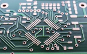
Several characteristics distinguish a Single-Layer Rigid-Flex PCB from more complex multilayer constructions.
Shielding
Shielding can be incorporated into the design to help control electromagnetic interference and protect sensitive signals. The appropriate shielding method depends on the electrical environment, signal frequency, and mechanical requirements.
Controlled Impedance
High-speed electronic systems may require controlled impedance to maintain signal integrity. Trace width, copper thickness, dielectric thickness, and material properties all influence impedance.
Although a single conductive layer limits routing options compared with multilayer designs, careful stack-up and trace geometry can still provide controlled electrical performance for suitable applications.
Panelization
Panelization allows multiple PCB units to be manufactured together before individual boards are separated.
Proper panel design can improve manufacturing efficiency and maintain board stability during assembly. Depending on the production method, boards may be connected through tabs, routing features, or other panelization structures.
Advantages of Non-Layered Rigid-Flex PCBs
Space and Weight Reduction
One of the most important advantages of a Non-Layered Rigid-Flex PCB is the ability to reduce the need for separate cables, wires, and connectors.
Fewer interconnection components can free up valuable internal space while reducing overall assembly weight. This is especially useful for compact electronic products where every millimeter of packaging space matters.
Faster Assembly
A rigid-flex structure can combine electrical interconnection and mechanical flexibility into one PCB solution.
Instead of installing separate rigid boards and cable assemblies, manufacturers can often reduce the number of assembly steps. This may simplify production and reduce opportunities for wiring mistakes.
For applications requiring component installation on flexible or rigid-flex circuits, GOPCBA also provides Rigid-Flex PCB Assembly solutions.
Improved Interconnection Reliability
Every connector, cable, and mechanical connection introduces another potential point of failure.
A properly designed rigid-flex PCB can reduce the number of electrical connection points and provide a more integrated interconnection structure. This can improve resistance to vibration, mechanical movement, and repeated environmental stress when the PCB is designed according to its operating conditions.
Better Resistance to Vibration
Flexible circuit sections can accommodate controlled movement and mechanical displacement.
This makes rigid-flex technology useful in products exposed to vibration, shock, or continuous mechanical movement. However, the flexible section must be designed with an appropriate bend radius and copper geometry to prevent excessive mechanical stress.
Simplified Testing
Because several electrical interconnections can be integrated into a single PCB structure, testing can be more straightforward than testing multiple separate boards connected through cables and connectors.
Electrical continuity testing, open-and-short testing, AOI, dimensional inspection, and other quality-control procedures can be applied according to the product requirements.
Limitations of Non-Layered Rigid-Flex PCBs
Although a Single-Layer Rigid-Flex PCB provides several advantages, it is not suitable for every application.
Limited Current-Carrying Capability
A single conductive layer provides fewer options for distributing current than a multilayer PCB.
For high-current applications, engineers may need thicker copper, wider traces, additional conductive layers, or a different PCB construction.
Greater Exposure to Mechanical Damage
Flexible circuits are thinner than conventional rigid boards and may be more sensitive to excessive bending, abrasion, environmental exposure, or improper handling.
Coverlay, stiffeners, protective films, and appropriate mechanical design can help improve durability.
Limited Routing Density
Single-layer flexible circuits provide fewer routing options than double-sided or multilayer flexible PCBs.
When a design requires complex signal routing, high component density, multiple ground planes, or high-speed interconnections, a multilayer rigid-flex structure may be more appropriate.
Materials Used in Non-Layered Rigid-Flex PCB Manufacturing
Material selection has a major impact on the electrical, thermal, and mechanical performance of a rigid-flex circuit.
Coverlay and Flexible Substrate
Common flexible materials include:
- Polyimide film
- Liquid photoimageable coverlay
- Flexible dielectric films
- Polyimide-glass structures for reinforced areas
Polyimide is widely used because of its flexibility, thermal stability, and suitability for flexible electronic applications.
Conductors
Copper is the primary conductor used in flexible circuits.
Copper thickness should be selected according to current requirements, mechanical bending conditions, impedance requirements, and manufacturing capability.
Adhesives
Depending on the PCB construction, adhesives may include:
- Polyimide adhesive systems
- Acrylic adhesives
- Epoxy adhesives
- Flame-retardant acrylic adhesives
- Epoxy-based bonding materials
The adhesive system should be selected based on temperature, flexibility, reliability, and environmental requirements.
Stiffeners
Stiffeners are commonly used to reinforce connector areas, component-mounting areas, and other sections that require additional mechanical strength.
Typical stiffener materials include:
- FR-4
- Polyimide
- Polyimide-glass
- Copper
- Aluminum
How Are Non-Layered Rigid-Flex PCBs Manufactured?
The manufacturing process for a Rigid-Flex PCB Manufacturing project requires careful control of materials, circuit geometry, lamination, drilling, surface treatment, and testing.
1. Material Preparation
The manufacturing process begins by preparing the copper-clad flexible material, coverlay, stiffeners, adhesives, and rigid materials required by the design.
Copper-clad laminates are cleaned and cut to the required production dimensions. Flexible films and reinforcement materials are also prepared according to the engineering drawings.
2. Flexible Circuit Formation
The flexible circuit pattern is transferred onto the copper surface using imaging and photolithographic processes.
After imaging, unwanted copper is removed through controlled etching, leaving the required conductive traces.
The resulting circuit pattern must meet the specified trace width, spacing, copper thickness, and dimensional tolerances.
3. Coverlay Application
A coverlay or suitable protective material is applied over the flexible circuit to protect copper traces from mechanical damage and environmental exposure.
Openings are created where solder pads, contacts, or other electrical connection points need to remain accessible.
4. Drilling
Depending on the PCB structure, mechanical drilling or laser drilling may be used to create holes.
The drilling process must consider hole diameter, positional accuracy, aspect ratio, flexible-area restrictions, and the requirements of the final assembly.
5. Rigid Section Formation
For rigid-flex constructions that include rigid sections, rigid PCB materials and bonding layers are integrated with the flexible circuit.
The lamination process must maintain accurate registration between rigid and flexible areas while controlling overall thickness and mechanical stress.
6. Removal of Unwanted Material
Additional prepreg or rigid material outside the intended flexible area may need to be removed.
This creates the required flexible region and ensures that the bending area remains mechanically compliant.
7. Surface Finish and Solder Mask
Exposed copper pads may receive a suitable surface finish to improve solderability and protect the copper from oxidation.
Depending on the application, surface finishes may include ENIG, OSP, HASL, immersion silver, immersion tin, ENEPIG, or other specified finishes.
Solder mask requirements can differ between rigid and flexible sections, so the material and process should be selected according to the PCB construction.
8. Electrical Testing and Inspection
The finished board should undergo appropriate inspection and electrical testing before shipment.
Typical quality-control processes may include:
- Automated optical inspection
- Electrical continuity testing
- Open-and-short testing
- Dimensional inspection
- Hole inspection
- Copper thickness verification
- Surface-finish inspection
- Solderability evaluation
- Functional testing where required
For projects requiring complete assembly and testing, PCB Assembly services can combine PCB fabrication with SMT, through-hole, and other assembly processes.
Design Considerations for Non-Layered Rigid-Flex PCBs
Successful Flexible PCB design requires both electrical and mechanical requirements to be considered from the beginning.
Avoid Vias and Pads in Bend Areas
Vias and component pads should generally be kept outside the dynamic bending area.
Placing rigid structures in a repeatedly bending section can concentrate mechanical stress and increase the risk of copper fatigue or other reliability problems.
Keep connection points in mechanically stable areas whenever possible.
Route Traces Carefully Through Flexible Areas
Trace geometry has a significant effect on flexing reliability.
Traces should generally run smoothly through the bend region instead of using sharp corners. Curved or gradual routing can help distribute mechanical stress more evenly.
Trace spacing should also remain consistent, and unnecessary copper features should be avoided in areas subjected to repeated bending.
Avoid Solid Copper Where Flexibility Is Required
A large solid copper area can increase stiffness in the flexible section.
For applications where mechanical flexibility is important, engineers may consider cross-hatched copper patterns or other appropriate grounding structures.
The exact solution should be determined according to electrical performance, EMI requirements, bend conditions, and manufacturing capability.
Consider Bend Radius
Bend radius is one of the most important mechanical design parameters.
The appropriate minimum bend radius depends on factors such as:
- Number of conductive layers
- Copper thickness
- Substrate thickness
- Static or dynamic bending
- Bend frequency
- Material characteristics
- Operating temperature
A flexible PCB should never be designed simply as a thinner version of a rigid PCB. Its mechanical behavior must be considered as part of the overall product design.
Applications of Non-Layered Rigid-Flex PCBs
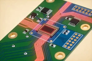
The compact size and mechanical flexibility of rigid-flex technology make it suitable for many electronic products.
Aerospace and Defense
Lightweight and compact circuit structures are valuable in aerospace electronics, avionics, communication equipment, radar systems, and other applications where space and weight are important.
For high-reliability applications, material selection, environmental testing, mechanical design, and manufacturing controls should be defined at the beginning of the project.
Automotive Electronics
Automotive products increasingly require compact electronic systems with fewer cables and connectors.
Rigid-flex circuits can be used in sensors, control modules, displays, lighting systems, camera modules, and other applications requiring compact electrical interconnections.
Consumer Electronics
Wearable devices, smartphones, cameras, headphones, portable electronics, and other compact products can benefit from flexible circuit technology.
The flexible section can follow product contours while rigid areas provide stable mounting locations for components.
Industrial Automation
Industrial equipment may require PCBs that can tolerate vibration while fitting around mechanical structures.
Rigid-flex circuits can be used in sensors, robotics, motion-control equipment, industrial instruments, and automation systems.
For industrial electronics requiring complete manufacturing and assembly support, GOPCBA also provides dedicated industrial PCBA solutions.
Medical Electronics
Compact electronic structures are increasingly important in medical instruments, diagnostic equipment, surgical systems, wearable medical devices, and other space-constrained applications.
Rigid-flex technology can help reduce wiring and improve mechanical integration while maintaining reliable electrical connections.
How to Avoid Common Non-Layered Rigid-Flex PCB Design Errors
Designing a Non-Layered Rigid-Flex PCB requires more than simply combining rigid and flexible materials.
Both electrical and mechanical engineering requirements must be considered.
Do Not Place Vias in the Bend Area
Avoid placing vias, plated holes, or component pads directly inside areas that will experience repeated bending.
Mechanical stress can be transferred into the copper and plated structures, potentially reducing long-term reliability.
Do Not Use Sharp Trace Corners
Sharp corners can concentrate mechanical stress in flexible areas.
Smooth routing and curved trace paths are generally preferable for flex regions.
Do Not Ignore Mechanical Requirements
The PCB must be evaluated together with the product enclosure, hinges, moving parts, connectors, mounting points, and assembly process.
Mechanical clearance should be verified before production.
Perform DFM Review Before Manufacturing
Early engineering review can identify potential issues with trace spacing, bend areas, material selection, holes, stiffeners, layer transitions, and assembly requirements.
GOPCBA supports engineering review and manufacturing analysis to help identify production risks before fabrication.
Future Development of Non-Layered Rigid-Flex Technology
Flexible and rigid-flex circuit technologies are expected to continue developing as electronic products become smaller, lighter, and more integrated.
Several trends are likely to influence future development.
More Applications
The demand for compact and flexible electronics is expanding across wearable electronics, IoT devices, automotive systems, robotics, medical electronics, and industrial equipment.
Improved Manufacturing Efficiency
Advances in materials, automation, imaging, drilling, lamination, and inspection technologies can improve production efficiency and manufacturing consistency.
More Advanced Design Tools
Modern PCB CAD and simulation tools can help engineers evaluate electrical performance, mechanical constraints, bend conditions, and manufacturability earlier in the product-development process.
Three-Dimensional Integration
As electronic products increasingly use three-dimensional mechanical structures, flexible circuits can provide electrical connections that follow curved or irregular product geometries.
This can create new opportunities for compact electronic packaging.
Advanced Materials
Future flexible PCB materials are expected to provide improved thermal stability, dimensional stability, electrical performance, and mechanical durability.
These developments may allow flexible circuits to operate reliably in increasingly demanding environments.
Why Choose GOPCBA for Rigid-Flex PCB Projects?
A reliable rigid-flex PCB supplier needs to understand both PCB fabrication and mechanical flexibility.
GOPCBA supports rigid, flexible, and rigid-flex PCB manufacturing together with PCB assembly capabilities, allowing customers to manage fabrication and assembly through one manufacturing partner.
Our capabilities cover prototype development, production manufacturing, SMT assembly, through-hole assembly, testing, and other electronic manufacturing requirements.
For customers developing a new rigid-flex product, early engineering communication is important. Providing Gerber or ODB++ files, stack-up information, fabrication drawings, BOM data, material specifications, and mechanical requirements can help engineers evaluate manufacturability before production.
For rapid development and prototype requirements, Rapid PCB Prototyping can help shorten the time between PCB design and functional verification.
Get a Quote for Your Rigid-Flex PCB Project
A Non-Layered Rigid-Flex PCB can be an effective solution when an electronic product requires compact packaging, reduced wiring, mechanical flexibility, and reliable electrical interconnection.
However, successful performance depends on appropriate material selection, trace routing, bend-radius design, rigid-to-flex transitions, manufacturing control, and testing.
Whether you need a single-sided flexible structure, a more advanced rigid-flex design, or complete PCB assembly, selecting the right manufacturing process at the beginning can help reduce production risks and improve product reliability.
Prepare your Gerber files, stack-up drawings, BOM, specifications, and mechanical requirements for engineering review, and contact GOPCBA for your rigid-flex PCB manufacturing and assembly project.