High-Speed PCB Design: Key Strategies for Signal Integrity and High-Performance Electronics
High-speed PCB design is essential for modern electronic systems that require fast data transmission, low latency, reliable power delivery, and excellent electromagnetic compatibility. From AI servers and telecommunications equipment to automotive electronics, industrial automation, aerospace systems, and IoT devices, increasingly higher data rates are placing greater demands on PCB design and manufacturing.
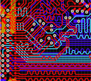
Although high-speed circuits are sometimes broadly associated with frequencies above 1 GHz, frequency alone does not determine whether a PCB should be treated as a high-speed design. In practical engineering, signal rise time, edge rate, interconnect length, transmission-line effects, and data rate are often more important factors.
When signal transitions are sufficiently fast, PCB traces can no longer be treated simply as ideal wires. They behave as transmission lines, making impedance control, return-path design, stackup configuration, routing topology, power integrity, and electromagnetic compatibility critical considerations.
A successful high-speed PCB design therefore requires close coordination between circuit design, simulation, PCB layout, fabrication, assembly, and testing.
What Is High-Speed PCB Design?
High-speed PCB design refers to the design and optimization of printed circuit boards that carry fast-changing digital or high-frequency signals while maintaining acceptable signal integrity, power integrity, and electromagnetic compatibility.
Unlike conventional low-speed PCB designs, high-speed designs must account for electrical effects that become significant when signal edge rates are fast relative to the propagation delay of the interconnect.
Typical high-speed interfaces include:
- PCIe
- DDR memory
- USB
- Ethernet
- HDMI and DisplayPort
- SerDes interfaces
- High-speed ADC/DAC interfaces
- High-speed networking interfaces
- AI accelerator interconnects
Common challenges include:
- Signal reflection
- Insertion loss
- Crosstalk
- Ground bounce
- Simultaneous switching noise
- Power supply noise
- Electromagnetic interference
- Timing skew
- Via discontinuities
- Thermal stress
The objective is not simply to make signals travel faster, but to ensure that signals arrive at their destinations with sufficient amplitude, timing accuracy, and waveform quality.
Key Considerations in High-Speed PCB Design
A reliable high-speed PCB requires a coordinated approach to signal integrity, power integrity, EMC, thermal management, and manufacturability.
1. Signal Integrity: Maintaining Accurate Data Transmission
Signal integrity is one of the most important aspects of high-speed PCB design.
As signal speeds increase, impedance discontinuities, reflections, crosstalk, dielectric loss, conductor loss, and timing variations can significantly degrade signal quality.
Controlled Impedance
Controlled impedance ensures that critical transmission lines maintain a predictable characteristic impedance.
Common impedance targets include:
- 50 Ω for many single-ended interfaces
- 90 Ω differential
- 100 Ω differential
- Other values specified by the interface standard
The actual impedance depends on the interface, PCB stackup, dielectric material, trace width, trace spacing, copper thickness, and reference-plane configuration.
Therefore, impedance should be designed together with the PCB stackup rather than determined only after routing is completed.
Minimize Signal Reflections
Reflections occur when a signal encounters an impedance discontinuity.
Common causes include:
- Incorrect trace width
- Improper termination
- Via transitions
- Connectors
- Layer changes
- Stubs
- Discontinuous reference planes
Reducing these discontinuities helps maintain waveform quality and minimize data errors.
Reduce Crosstalk
Crosstalk occurs when electromagnetic energy from one signal trace couples into a neighboring trace.
Crosstalk can be reduced by:
- Increasing spacing between sensitive traces
- Maintaining an appropriate reference plane
- Controlling parallel routing length
- Using differential signaling where appropriate
- Avoiding unnecessary routing through sensitive areas
- Maintaining proper stackup geometry
For particularly sensitive signals, routing strategy should be evaluated using electromagnetic or signal-integrity simulation.
2. Power Integrity: Providing a Stable Power Supply
Power integrity (PI) is equally important in high-speed PCB systems.
Modern processors, memory devices, FPGAs, GPUs, and AI accelerators can switch large amounts of current within extremely short time intervals. If the power distribution network cannot respond quickly enough, voltage fluctuations and power noise can occur.
A well-designed power distribution network (PDN) should provide stable power with low impedance across the relevant frequency range.
Decoupling Capacitors
Decoupling capacitors help supply transient current close to the power pins of integrated circuits.
Their effectiveness depends on more than simply increasing capacitance. Designers should consider:
- Capacitor value
- Equivalent series resistance (ESR)
- Equivalent series inductance (ESL)
- Mounting location
- Via structure
- Power and ground plane geometry
- Target frequency range
Placing suitable capacitors close to device power pins can reduce high-frequency power fluctuations and improve system stability.
Low-Inductance Power Delivery
High-speed systems are highly sensitive to parasitic inductance.
Short current paths, optimized via structures, solid reference planes, and appropriate power/ground distribution can help reduce unwanted inductance.
For high-current applications, additional copper thickness, copper planes, thermal vias, and embedded copper structures may be considered.
3. Electromagnetic Compatibility: Controlling EMI and EMC
High-speed signals can generate significant electromagnetic energy, especially when signal edges are extremely fast.
Poor PCB layout can cause excessive electromagnetic emissions or make the system more susceptible to external interference.
Effective EMC design strategies include:
- Maintaining continuous reference planes
- Controlling return-current paths
- Minimizing unnecessary loop areas
- Separating noisy and sensitive circuits
- Optimizing connector placement
- Controlling high-speed layer transitions
- Using appropriate shielding and grounding techniques
- Applying common-mode filtering where required
Ground and Reference Planes
A continuous reference plane provides a low-impedance return path for high-frequency currents.
If a high-speed trace crosses a split or discontinuity in its reference plane, the return current may be forced to take a longer path, increasing loop area and potentially increasing EMI.
Therefore, high-speed routing should be planned together with the return path rather than treating signal traces independently.
Via Placement
Vias can introduce parasitic capacitance and inductance and may create impedance discontinuities.
When a high-speed signal changes layers, the associated return path must also be considered.
In some designs, strategically placed ground vias can help maintain return-current continuity and reduce unwanted electromagnetic coupling.
Optimizing the High-Speed PCB Stackup
The PCB stackup is one of the most important elements of a high-speed design.
A properly engineered stackup establishes the relationship between signal layers, reference planes, dielectric thickness, copper thickness, and power distribution.
Layer Selection
The required number of PCB layers depends on:
- Signal count
- Routing density
- Power distribution requirements
- High-speed interface count
- EMI requirements
- Thermal requirements
- Mechanical constraints
A multilayer PCB can provide dedicated signal layers and continuous reference planes, making it easier to control impedance and signal return paths.
Dielectric Material Selection
The PCB material directly affects signal propagation and loss.
Important material parameters include:
- Dielectric constant (Dk)
- Dissipation factor (Df)
- Glass transition temperature (Tg)
- Coefficient of thermal expansion (CTE)
- Moisture resistance
- Thermal conductivity
For high-speed applications, low-loss materials may be preferred when conventional FR-4 materials cannot provide the required electrical performance.
Materials such as PTFE-based laminates, low-loss FR-4 variants, and specialized high-frequency laminates from manufacturers such as Rogers may be considered depending on the application.
Material selection should be based on the actual signal frequency range, insertion-loss requirements, manufacturing capability, cost, and reliability requirements.
Advanced Routing Techniques for High-Speed Signals
Routing is critical to maintaining signal integrity.
Differential Pair Routing
Differential signaling uses two complementary traces to transmit information.
High-speed differential pairs should generally maintain:
- Controlled differential impedance
- Consistent spacing
- Appropriate trace width
- Controlled skew
- Continuous reference planes
- Minimal unnecessary vias
The two traces should remain geometrically consistent through the majority of the routing path.
However, exact matching should follow the requirements of the specific interface rather than assuming that every differential pair must have exactly the same physical length.
Minimize Via Usage
Vias can introduce discontinuities and additional parasitic effects.
For high-speed interfaces, unnecessary vias should be minimized.
When appropriate, designers may use:
- Blind vias
- Buried vias
- Microvias
- Back-drilled vias
Back-drilling can be particularly useful for reducing long via stubs in high-speed multilayer designs.
Keep Critical Interconnects Short
Longer traces generally introduce additional propagation delay and loss.
For high-speed interfaces, critical signal paths should be kept as short as practical while maintaining correct topology, impedance, and routing constraints.
However, the shortest route is not always the best route. A slightly longer route with a continuous reference plane and controlled impedance can perform better than a shorter route with severe discontinuities.
Advanced Technologies for High-Speed PCB Design
1. High-Density Interconnect (HDI)
HDI PCB technology enables higher routing density through fine lines, microvias, sequential lamination, and optimized layer structures.
HDI is particularly useful for:
- Smartphones
- AI accelerator modules
- Compact computing systems
- High-density networking equipment
- Advanced automotive electronics
- Miniaturized industrial systems
Microvias can reduce routing congestion and enable more efficient interconnection between layers.
2. Modified Semi-Additive Process (mSAP)
mSAP technology enables very fine circuit features and is widely associated with advanced high-density PCB manufacturing.
Fine-line fabrication can support compact routing structures and high I/O density, particularly when conventional subtractive processing reaches its practical limits.
The actual achievable trace width and spacing depend on the PCB material, copper thickness, fabrication process, equipment capability, and design rules.
3. Copper Inlay for High-Current Applications
High-performance processors, VRMs, GPUs, AI accelerators, and power electronics can generate significant heat and current.
Copper inlay or embedded copper structures can provide:
- Lower electrical resistance
- Improved current-carrying capability
- Better heat spreading
- Reduced localized temperature rise
This technology is particularly valuable in high-current regions where conventional copper thickness may not provide sufficient electrical or thermal performance.
Common Challenges in High-Speed PCB Design
Signal Reflection and Insertion Loss
Impedance discontinuities, excessive via stubs, connectors, long traces, and unsuitable materials can increase signal loss and reflection.
For demanding interfaces, designers should evaluate the entire interconnect channel rather than only the PCB trace.
Crosstalk
High-density routing increases the possibility of capacitive and inductive coupling between adjacent signals.
Trace spacing, routing direction, reference planes, and layer assignment should therefore be considered during stackup planning.
Thermal Management
Modern processors and AI devices can generate substantial heat.
High-speed PCB design must therefore consider:
- Copper distribution
- Thermal vias
- Heat spreaders
- Copper inlays
- Component placement
- Airflow
- Thermal interface materials
- PCB material thermal characteristics
Signal integrity and thermal management should be treated as interconnected design requirements.
Cost and Manufacturability
Advanced materials, HDI structures, low-loss laminates, fine-line fabrication, sequential lamination, back-drilling, and complex stackups can significantly increase manufacturing costs.
A successful design therefore balances:
Performance + Reliability + Manufacturability + Cost
Designers should involve the PCB manufacturer early in the development process to establish realistic design rules and manufacturing capabilities.
High-Speed PCB Simulation and Design Tools
Modern ECAD and simulation tools can significantly improve the reliability of high-speed PCB development.
Common tools and platforms include:
- Altium Designer for PCB design, routing, stackup planning, and design-rule management
- Cadence Allegro X / Sigrity for PCB design and signal/power integrity analysis
- Siemens Xpedition for advanced PCB layout and system-level design
- Ansys simulation solutions for electromagnetic, signal-integrity, and thermal analysis
Simulation can help identify problems before prototype fabrication.
Typical analysis includes:
- Signal integrity simulation
- Power integrity analysis
- S-parameter analysis
- Crosstalk analysis
- TDR analysis
- Eye-diagram analysis
- Thermal simulation
- Electromagnetic simulation
For complex high-speed interfaces, simulation should ideally be performed before PCB fabrication so that potential design problems can be corrected at a lower cost.
High-Speed PCB Design for AI Servers and GPU Systems
AI servers and GPU clusters place extraordinary demands on PCB performance.
These systems require high-bandwidth communication between processors, memory, storage, networking components, and accelerator devices.
A high-speed PCB for AI infrastructure may need to support:
- High-speed SerDes links
- High-speed memory
- High-current power delivery
- High-density interconnects
- Advanced thermal management
- Low-loss transmission channels
As data rates increase, PCB material selection, stackup design, connector performance, via structures, and power integrity become increasingly important.
High-Speed PCB Applications
1. AI Servers and GPU Clusters
AI servers require high-speed interconnects and high-current power delivery to support GPUs, CPUs, memory, networking devices, and accelerators.
The PCB must combine high routing density with controlled impedance, excellent thermal performance, and reliable power distribution.
2. Edge AI Accelerator Modules
Edge AI systems require real-time data processing with limited power and physical space.
High-speed PCB technology allows compact accelerator modules to integrate processors, memory, sensors, communication interfaces, and power-management circuits.
3. Automotive AI Computing
Automotive AI computing platforms process large volumes of sensor data for applications such as advanced driver assistance systems (ADAS), computer vision, sensor fusion, and autonomous driving.
These systems require high-speed communication, robust thermal management, electromagnetic compatibility, and long-term reliability.
4. Industrial Robot Controllers
Industrial robots rely on fast communication between processors, motor controllers, sensors, and control systems.
High-speed PCB design helps maintain low-latency communication while supporting high-density component placement and reliable operation in demanding industrial environments.
5. AI Inference and Accelerator Cards
AI inference cards require high-bandwidth connections between processors, memory, networking interfaces, and host systems.
PCB design must therefore provide controlled high-speed channels, stable power delivery, and efficient heat dissipation.
6. UAV and Aerospace AI Systems
Unmanned aerial vehicles and aerospace AI systems require compact and lightweight electronics with high processing capability.
High-speed PCB technology supports real-time sensor processing, communication, navigation, flight control, and AI-based decision-making while maintaining strict size, weight, power, and reliability requirements.
Best Practices for High-Speed PCB Layout
A practical high-speed PCB layout strategy should include the following:
- Define high-speed interfaces early in the design process.
- Develop the PCB stackup before detailed routing.
- Establish impedance requirements for critical interfaces.
- Maintain continuous reference planes.
- Control differential-pair geometry and skew.
- Minimize unnecessary vias and via stubs.
- Keep high-speed signal paths short and direct.
- Separate sensitive circuits from noisy power or switching circuits.
- Optimize decoupling capacitor placement.
- Perform signal and power integrity simulations before fabrication.
- Verify manufacturability with the PCB manufacturer.
- Use appropriate inspection and testing after assembly.
Following these principles can significantly reduce the risk of expensive prototype iterations and field failures.
Frequently Asked Questions About High-Speed PCB Design
1. What is considered a high-speed PCB?
There is no universal frequency threshold that defines every high-speed PCB. In practice, signal rise time, edge rate, interconnect length, transmission-line effects, and interface data rate are important factors. A relatively low-frequency signal with an extremely fast edge can still require high-speed PCB design techniques.
2. Why is impedance control important in high-speed PCB design?
Controlled impedance helps minimize reflections and preserve signal quality. It is particularly important for high-speed interfaces where impedance discontinuities can cause waveform distortion, timing errors, and communication failures.
3. Which PCB materials are suitable for high-speed applications?
Material selection depends on frequency, data rate, insertion-loss requirements, thermal conditions, and cost. Low-loss FR-4 materials can be suitable for many applications, while PTFE-based and other specialized low-loss laminates may be preferred for more demanding high-frequency designs.
4. What role does HDI play in high-speed PCB design?
HDI enables fine-line routing and microvia structures, allowing designers to achieve greater routing density in compact form factors. It can be especially valuable for advanced computing, mobile, automotive, and AI applications.
5. How can signal integrity problems be reduced?
Common approaches include controlled impedance, continuous reference planes, optimized differential routing, reduced via stubs, appropriate termination, shorter critical paths, and pre-layout or post-layout simulation.
6. How can crosstalk be reduced?
Crosstalk can be reduced by increasing spacing between sensitive traces, limiting parallel routing, maintaining an appropriate reference plane, optimizing layer assignment, and separating noisy signals from sensitive circuits.
7. Why are vias a concern in high-speed PCB design?
Vias introduce parasitic capacitance and inductance and may create impedance discontinuities. Long via stubs can also cause resonances at high frequencies. Techniques such as microvias and back-drilling can help reduce these effects when required.
8. Why is power integrity important for high-speed systems?
High-speed processors can experience rapid changes in current demand. An improperly designed PDN can produce voltage noise and transient fluctuations that affect device stability and signal quality.
9. How does thermal management affect high-speed PCB design?
High-performance processors and power devices generate substantial heat. Excessive temperature can affect component reliability, material properties, and electrical performance. Thermal vias, copper planes, heat spreaders, copper inlays, and appropriate component placement can help control temperature.
10. Why is simulation important before manufacturing a high-speed PCB?
Simulation allows designers to identify potential signal-integrity, power-integrity, electromagnetic, and thermal problems before building physical prototypes. Early detection can reduce redesign cycles, manufacturing costs, and development time.
Conclusion
High-speed PCB design is a multidisciplinary engineering process that combines signal integrity, power integrity, EMC, thermal management, materials engineering, PCB layout, simulation, and manufacturing expertise.
As AI servers, high-performance computing, automotive electronics, telecommunications, industrial automation, and aerospace systems continue to demand higher bandwidth and lower latency, PCB designs must handle increasingly fast signal transitions and higher power densities.
Effective high-speed design begins with the right architecture and stackup, followed by controlled impedance routing, optimized return paths, appropriate materials, careful via design, robust power distribution, and comprehensive simulation.
For advanced applications, technologies such as HDI PCB, mSAP, low-loss laminates, back-drilling, microvias, and copper inlays can further improve routing density, electrical performance, and thermal management.
Kingda can support high-performance electronics projects with integrated PCB manufacturing and PCB assembly capabilities, helping customers translate high-speed design requirements into manufacturable and reliable electronic products.