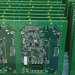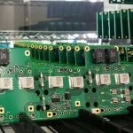
What Is the PCB Manufacturing Process?
The PCB Manufacturing Process is a series of controlled manufacturing steps used to transform electronic design data and copper-clad materials into a finished printed circuit board. Depending on the board structure, layer count, material, copper thickness, via technology, and performance requirements, the exact process may vary.
A typical PCB fabrication workflow includes engineering review, material preparation, inner-layer imaging and etching, lamination, drilling, copper plating, outer-layer imaging and etching, solder mask application, surface finishing, electrical testing, and final inspection.
For advanced boards, additional processes such as laser drilling, via filling, impedance control, sequential lamination, and specialized surface finishes may also be required.
For projects requiring both board fabrication and assembly, PCB Manufacturing Services can be integrated with downstream PCBA production to simplify the manufacturing process.
How Does PCB Manufacturing Work?
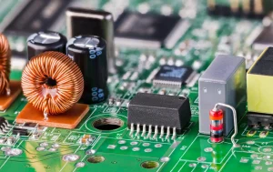
The manufacturing process begins with the customer’s Gerber files, drill files, stack-up information, fabrication drawings, and other technical documentation. Before production starts, engineers verify whether the design can be manufactured consistently and whether the specified materials and processes are appropriate.
The major stages are outlined below.
1. Engineering Review and DFM Analysis
Before physical production begins, engineers review all manufacturing data supplied by the customer.
The engineering review normally covers:
- Gerber and ODB++ data
- PCB dimensions and panelization
- Layer stack-up
- Trace width and spacing
- Drill sizes and tolerances
- Via structures
- Copper thickness
- Material specifications
- Surface finish
- Solder mask and silkscreen
- Impedance requirements
- Special manufacturing requirements
Design for Manufacturing (DFM) analysis is particularly important for complex and high-density circuit boards. Potential problems can be identified before production, reducing the risk of manufacturing defects, delays, and unnecessary redesigns.
A professional manufacturer can also review the design together with the assembly requirements when the project requires complete PCB Assembly Services.
2. Material Preparation and Panel Cutting
After engineering approval, the appropriate raw materials are selected according to the PCB specification.
Common PCB materials include FR-4, high-Tg materials, Rogers materials, aluminum-backed materials, flexible materials, and rigid-flex materials. Material selection depends on electrical, thermal, mechanical, and environmental requirements.
The copper-clad laminate is then cut into production panels according to the required board dimensions and manufacturing panel layout.
For multilayer boards, individual copper-clad cores and prepreg materials are prepared for subsequent layer stacking.
3. Inner Layer Imaging
For a multilayer PCB, the inner copper layers must first be formed individually.
The copper surface is cleaned to remove contaminants and improve photoresist adhesion. A photosensitive dry film is then laminated onto the copper surface.
The circuit image is transferred onto the dry film using ultraviolet exposure. Modern PCB factories may use Laser Direct Imaging (LDI) technology to improve pattern accuracy, particularly for fine-line and high-density PCB designs.
After exposure, the panel is developed. The unwanted portions of the photoresist are removed, leaving the required circuit pattern protected.
4. Inner Layer Etching and AOI Inspection
The exposed copper is removed through a controlled chemical etching process. Copper protected by the remaining photoresist forms the required circuit traces and pads.
After etching, the inner layers are inspected using Automated Optical Inspection (AOI).
AOI compares the manufactured circuit pattern with the original design data to identify potential defects such as:
- Open circuits
- Short circuits
- Missing copper
- Excess copper
- Incorrect trace geometry
- Pattern defects
This inspection stage helps prevent defective inner layers from entering the lamination process.
5. Oxide Treatment and Layer Lamination
After inner-layer inspection, the copper surfaces are treated to improve bonding between the copper and dielectric materials.
The prepared inner layers are then stacked together with prepreg and copper foil according to the specified layer structure.
Precise alignment is essential during this stage because even a small layer-registration error can affect vias, pads, impedance, and overall circuit performance.
The stack-up is placed into a lamination press. Under carefully controlled temperature and pressure, the prepreg softens and flows between the layers before curing into a solid dielectric structure.
The result is a multilayer PCB panel with the internal circuits permanently bonded together.
6. Mechanical and Laser Drilling
After lamination, holes are drilled according to the customer’s drill data.
Mechanical drilling is commonly used for standard through-holes and larger via structures. Advanced multilayer boards may also require laser drilling for microvias and high-density interconnect structures.
Depending on the design, the PCB may contain:
- Through holes
- Blind vias
- Buried vias
- Microvias
- Via-in-pad structures
- Tooling holes
Drilling accuracy is critical because the holes must connect the intended copper layers correctly.
For high-density designs, HDI PCB Manufacturing can incorporate laser drilling and advanced via structures to support smaller features and tighter routing requirements.
7. Deburring and Hole Cleaning
Mechanical drilling can produce burrs and debris around the drilled holes. These contaminants must be removed before the plating process.
The panels undergo cleaning and desmear processes to remove drilling residue and prepare the hole walls for reliable copper deposition.
Proper hole preparation is particularly important for multilayer boards because the copper deposited inside the holes must establish reliable electrical connections between layers.
8. Electroless Copper Plating
After hole preparation, the panel undergoes chemical treatment to deposit a thin layer of conductive copper onto the hole walls and exposed surfaces.
This electroless copper layer provides the conductive foundation required for subsequent electroplating.
The process creates a continuous conductive path through the drilled holes, allowing additional copper to be built up during the next plating stage.
9. Outer Layer Imaging
Once the initial copper deposition is complete, the outer circuit pattern is created.
The panel is cleaned and laminated with photosensitive dry film. The desired circuit image is transferred onto the dry film through UV exposure or LDI.
The panel is then developed to expose the copper areas that need to be plated.
This stage determines the final geometry of the external circuit traces, pads, and other copper features.
10. Copper Pattern Plating
The prepared panel is placed into an electroplating system.
Additional copper is deposited onto the exposed circuit areas and inside the plated holes. The plating thickness is controlled according to the customer’s specifications and applicable manufacturing requirements.
For advanced PCB designs, copper thickness must be carefully controlled because it affects electrical conductivity, thermal performance, impedance, and manufacturing tolerances.
After copper plating, a protective metal layer may be applied to protect the desired copper pattern during subsequent etching.
11. Resist Stripping and Outer Layer Etching
After pattern plating, the dry film is stripped from the panel.
The exposed unwanted copper is then removed through controlled chemical etching, while the protected circuit areas remain intact.
The etching process must be carefully controlled. Excessive etching can reduce trace width, while insufficient etching may leave unwanted copper and cause electrical shorts.
After etching, the remaining protective material is removed, leaving the completed outer-layer circuit pattern.
12. Solder Mask Application
A solder mask is applied over the PCB surface to provide electrical insulation and protect copper from environmental contamination and accidental solder bridging.
The solder mask is typically applied across the board and then exposed and developed to open the areas that require soldering, such as component pads, test points, and selected through-hole locations.
After development, the board is cured under controlled conditions.
Solder mask colors can vary depending on customer requirements, although green remains one of the most widely used options.
13. Surface Finish
The exposed copper pads require a suitable surface finish to protect the copper and provide a reliable soldering surface.
Common PCB surface finishes include:
- ENIG
- HASL
- Lead-free HASL
- OSP
- Immersion Tin
- Immersion Silver
- ENEPIG
- Hard Gold
The appropriate finish depends on component technology, soldering requirements, storage conditions, electrical performance, contact requirements, and cost considerations.
For example, ENIG is widely used for fine-pitch components and applications requiring a flat soldering surface, while hard gold is commonly selected for edge contacts and other wear-resistant applications.
14. Silkscreen and Marking
The next stage is applying component references, polarity indicators, logos, identification codes, and other required markings.
Silkscreen can be applied using traditional screen printing or modern digital printing technology.
Accurate markings help operators during assembly and inspection while also providing useful identification information for manufacturing and servicing.
15. Electrical Testing
Before shipment, finished PCBs undergo electrical testing to verify circuit continuity and isolation.
Electrical testing can identify problems such as:
- Open circuits
- Short circuits
- Incorrect connections
- Electrical isolation failures
Depending on the PCB design and customer requirements, manufacturers may use flying-probe testing, fixture-based testing, or other automated electrical test methods.
Electrical testing is an important part of overall PCB quality assurance because visual inspection alone cannot identify every electrical defect.
16. Final Inspection and Quality Control
After electrical testing, the finished boards undergo final inspection.
Quality control may include:
- Dimensional inspection
- Visual inspection
- Copper thickness verification
- Surface finish inspection
- Solder mask inspection
- Silkscreen verification
- Hole and via inspection
- Electrical testing
- Impedance testing when required
- Packaging inspection
Manufacturing records and inspection results can also be maintained for traceability.
For projects involving complete electronic manufacturing, PCB fabrication can be combined with PCBA Capabilities such as SMT, through-hole assembly, inspection, and functional testing.
PCB Manufacturing Process for Multilayer Boards
The manufacturing process becomes more complex as the number of PCB layers increases.
A typical multilayer PCB may include multiple signal layers, power planes, and ground planes separated by dielectric materials.
Advanced multilayer designs can also incorporate:
- High-Tg materials
- Controlled impedance
- Blind and buried vias
- Microvias
- Via-in-pad
- Sequential lamination
- Heavy copper
- High-frequency materials
- High-speed signal structures
These technologies require tighter process control because layer registration, dielectric thickness, copper thickness, drilling accuracy, and impedance performance are closely interconnected.
What Determines PCB Manufacturing Cost?
PCB manufacturing cost depends on more than board dimensions.
Important cost factors include:
- Number of PCB layers
- Board dimensions
- Material type
- Copper thickness
- Minimum trace and spacing
- Minimum drill diameter
- Number and type of vias
- Surface finish
- PCB quantity
- Manufacturing lead time
- Special impedance requirements
- Testing requirements
- Panel utilization
- Additional processes such as laser drilling or via filling
For example, a simple two-layer FR-4 PCB with standard HASL finish can be significantly less expensive than a high-layer-count HDI PCB using high-performance laminate, microvias, controlled impedance, and ENIG.
How to Choose a PCB Manufacturing Partner
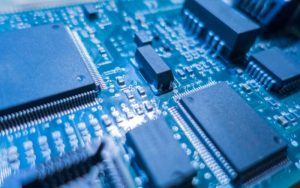
Selecting the right PCB supplier is important for both prototype development and long-term production.
A capable PCB manufacturer should provide:
- Engineering and DFM support
- Stable material sourcing
- Advanced PCB fabrication capabilities
- Reliable drilling and plating processes
- Automated inspection
- Electrical testing
- Traceability
- Consistent quality control
- Flexible production quantities
- Responsive technical support
It is also useful to verify whether the supplier can support both PCB fabrication and assembly. A one-stop manufacturing partner can reduce communication between multiple suppliers and simplify project management.
For customers evaluating manufacturing partners, Why Choose Us provides additional information about manufacturing qualifications, certifications, and quality capabilities.
From PCB Fabrication to Complete PCBA Manufacturing
PCB fabrication is only one part of the electronic product manufacturing process.
Once the bare PCB has passed inspection, it can move to component assembly. Depending on the product requirements, this may involve solder paste printing, SMT component placement, reflow soldering, through-hole assembly, AOI, X-ray inspection, ICT, functional testing, and final inspection.
A complete manufacturing workflow can therefore be summarized as:
Engineering Review → PCB Fabrication → Electrical Testing → Component Procurement → SMT/THT Assembly → Inspection → Functional Testing → Final Assembly → Packaging
For products requiring complete system integration, the manufacturing process can extend further into cable integration, mechanical assembly, enclosure installation, system testing, and finished-product packaging.
Why Process Control Matters in PCB Manufacturing
A high-quality PCB is the result of consistent control throughout the entire production cycle rather than a single manufacturing operation.
Material selection affects electrical and thermal performance. Imaging and etching determine circuit accuracy. Lamination affects layer registration and dielectric structure. Drilling and plating determine interlayer connectivity. Surface finishing affects solderability and long-term reliability. Electrical testing verifies that the finished board performs according to the required circuit design.
For this reason, an experienced PCB Manufacturing partner should combine engineering expertise, modern equipment, process monitoring, inspection systems, and documented quality procedures.
Conclusion
The PCB Manufacturing Process involves a carefully controlled sequence of engineering, material preparation, imaging, etching, lamination, drilling, plating, solder mask application, surface finishing, testing, and final inspection.
From simple single- and double-sided boards to advanced multilayer, HDI, high-frequency, rigid-flex, and heavy-copper designs, every PCB requires a manufacturing process matched to its electrical, mechanical, thermal, and reliability requirements.
Choosing a manufacturer with integrated engineering, fabrication, inspection, and assembly capabilities can help reduce production risks, improve consistency, and accelerate the transition from PCB design to finished electronic products.
For a complete manufacturing solution, PCB Manufacturing can be combined with PCB assembly, component sourcing, testing, and final product integration to create a streamlined electronics manufacturing workflow.