PCB Assembly Process: 8 Essential Steps
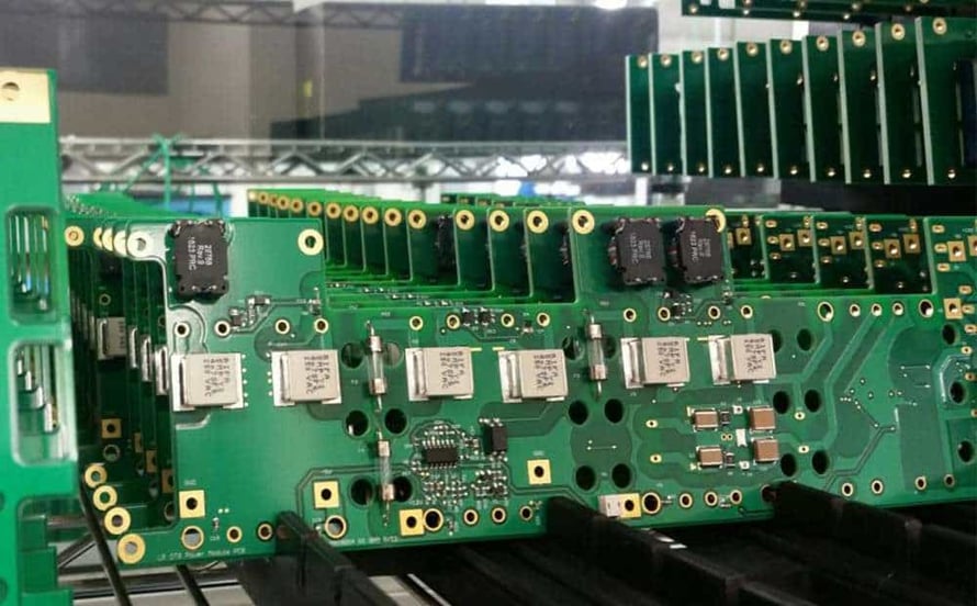
The PCB Assembly Process involves much more than simply placing components onto a printed circuit board. A reliable PCBA workflow combines engineering review, material preparation, SMT assembly, through-hole assembly, inspection, testing, quality control, labeling, and protective packaging.
For manufacturers handling prototype, low-volume, and high-volume production, each stage must be carefully controlled to ensure assembly accuracy, soldering quality, product reliability, and delivery consistency.
A professional PCB Assembly manufacturer typically integrates engineering support, component sourcing, PCB fabrication, assembly, inspection, and testing into a streamlined production process. GoPCBA provides one-stop PCB manufacturing and assembly solutions covering PCB fabrication, component procurement, SMT/THT assembly, testing, and final product integration.
Step 1: Prepare PCB Assembly Files
The first stage of the PCB Assembly Process is preparing and reviewing all production files. Complete and accurate documentation allows engineers to identify potential manufacturing and assembly problems before production begins.
Required PCB Assembly Files
The primary files normally required for PCB assembly include:
- Gerber files
- Bill of Materials (BOM)
- Pick-and-Place files
- PCB drawings
- Assembly drawings
- Schematic diagrams
- Component datasheets
- Special manufacturing or testing instructions
Gerber files contain the information required to manufacture the PCB and prepare SMT stencils. They also allow engineers to compare PCB pads, component footprints, solder mask openings, and other board details during the engineering review.
The BOM provides essential component information, including manufacturer, manufacturer part number, component description, package type, quantity, and approved alternatives.
Pick-and-Place files provide X/Y coordinates, component references, rotation angles, and placement information required by automated SMT equipment.
For customers who need PCB fabrication and assembly from a single supplier, PCB Manufacturing can be integrated with the assembly process to simplify project management and improve production consistency.
DFA and DFM Review
Before production, engineers should perform Design for Assembly (DFA) and Design for Manufacturing (DFM) checks.
Typical issues identified during this stage include:
- Incorrect component footprints
- PCB pad and component size mismatches
- Incorrect BOM quantities
- Obsolete or unavailable components
- Incorrect component part numbers
- Missing components
- Polarity inconsistencies
- Assembly clearance problems
- Incorrect Pick-and-Place coordinates
Early engineering review reduces the risk of production delays, component shortages, soldering problems, and costly rework.
Generate Production Documents
After the engineering review is completed, production documentation can be prepared. Depending on the project, production instructions may include solder paste requirements, reflow profiles, component placement information, THT assembly instructions, inspection requirements, testing procedures, programming instructions, conformal coating specifications, and packaging requirements.
A well-defined production package provides operators and quality engineers with consistent instructions throughout the entire manufacturing process.
Step 2: SMT PCB Assembly
SMT PCB Assembly is one of the most important stages of modern electronic manufacturing. Surface Mount Technology allows manufacturers to place a large number of components onto compact PCB designs while supporting high production efficiency and repeatable assembly quality.
GoPCBA provides SMT assembly for complex PCB designs and supports prototype, low-volume, and larger-scale production requirements. Its stated capabilities include fine-pitch packages, BGA, QFN, CSP, LGA, PoP, and miniature components.
Prepare the SMT Stencil
An SMT stencil is used to transfer solder paste onto PCB pads. Laser-cut stainless-steel stencils are commonly selected because they provide accurate and repeatable solder paste deposition.
Stencil thickness and aperture design depend on PCB design, component package, pad geometry, and solder paste requirements. Fine-pitch components may require specially optimized aperture designs to control solder volume and prevent bridging.
Prepare Pick-and-Place Data
The Pick-and-Place file is loaded into the SMT placement system to define the position and orientation of every component.
Engineers verify component references, coordinates, rotation, feeder assignments, and package information before production. Accurate placement data is particularly important for dense PCB layouts and fine-pitch components.
Prepare Production Fixtures
Some PCB designs require special fixtures or carriers during assembly.
For example, thin, flexible, unusually shaped, or poorly supported PCBs may require a custom carrier to prevent board movement or deformation during solder paste printing and component placement.
Fixtures can also improve repeatability when the PCB has limited edge clearance or unusual mechanical characteristics.
Apply Solder Paste
During solder paste printing, the stencil is aligned with the PCB and solder paste is transferred through the stencil openings onto the PCB pads.
Solder paste printing must be carefully controlled because insufficient, excessive, or misaligned solder paste can lead to defects such as:
- Solder bridges
- Insufficient solder
- Excess solder
- Open solder joints
- Component displacement
- Solder ball formation
After printing, solder paste inspection (SPI) can be used to verify paste volume, height, area, and position before component placement.
Place Components
Automated pick-and-place equipment places surface-mount components onto the solder-pasted PCB.
Modern SMT assembly lines can support a broad range of component packages, including miniature passive components, BGA, QFN, QFP, CSP, LGA, and other fine-pitch devices.
During production, operators and process engineers monitor feeder loading, component verification, placement accuracy, and equipment performance to minimize placement errors.
First Article Inspection
First Article Inspection (FAI) is especially important for new products, revised PCB designs, and new production runs.
The first assembled PCB is carefully inspected to verify:
- Correct component placement
- Component orientation
- Component value
- Reference designator
- Soldering condition
- Assembly configuration
- PCB revision
Only after the first article meets the required specifications should the remaining production quantity proceed.
Reflow Soldering
After component placement, the PCB passes through a reflow soldering oven.
A typical reflow profile consists of several temperature stages, including:
- Preheating
- Soaking
- Reflow
- Cooling
The temperature profile must be optimized according to the solder paste, PCB construction, component specifications, and customer requirements.
AOI Inspection
Automated Optical Inspection (AOI) uses cameras and image-processing technology to identify visible assembly defects.
AOI can detect issues such as:
- Missing components
- Incorrect components
- Component misalignment
- Polarity errors
- Solder bridges
- Insufficient solder
- Other visible soldering defects
AOI is an important part of modern PCB Assembly quality control because it provides fast and repeatable inspection after SMT soldering.
Step 3: Through-Hole PCB Assembly
Not every electronic component is suitable for surface mounting. Some products require components with leads inserted through PCB holes. This process is known as Through-Hole Technology (THT) or PTH assembly.
GoPCBA provides Through-Hole PCB Assembly using both manual and automated insertion methods, with capabilities including lead-free soldering, wave soldering, selective soldering, inspection, and functional testing.
Prepare Fixtures
Fixtures may be required to support the PCB during through-hole soldering.
They can protect sensitive components, maintain board stability, and prevent PCB deformation during thermal processing.
Insert Through-Hole Components
Through-hole components can be inserted manually or automatically depending on component type, product volume, and design requirements.
Typical THT components include:
- Connectors
- Relays
- Transformers
- Large capacitors
- Power components
- Switches
- Mechanical components
Component leads may also need to be formed or trimmed before soldering.
Wave or Selective Soldering
After component insertion, the PCB can pass through wave soldering or selective soldering equipment.
Wave soldering exposes the underside of the PCB to molten solder, allowing solder to flow through the plated holes and form reliable solder joints.
Selective soldering provides more localized soldering for through-hole components on boards that also contain sensitive SMT components.
Trim Excess Leads
After soldering, excess component leads may need to be trimmed. Proper lead trimming improves board appearance, reduces mechanical interference, and ensures the assembly meets dimensional requirements.
THT Quality Inspection
The completed THT assembly should be inspected for:
- Solder bridges
- Insufficient solder
- Cold solder joints
- Component polarity errors
- Incorrect component placement
- Open circuits
- Mechanical defects
For mixed-technology products, SMT and THT processes are normally combined into a controlled production flow. GoPCBA also offers Mixed Technology PCB Assembly for products requiring both surface-mount and through-hole components.
Step 4: Manual Assembly and Soldering
Although automated manufacturing covers most modern PCB assembly operations, manual assembly remains necessary for certain components and specialized production requirements.
Manual soldering may be used for:
- Complex through-hole components
- Large connectors
- Wires and cables
- Rework
- Engineering prototypes
- Low-volume production
- Components that cannot be processed automatically
Manual soldering requires trained operators and controlled soldering temperatures. Operators must follow standardized work instructions to maintain consistent solder joint quality.
Manual assembly should complement automated production rather than replace controlled SMT and THT processes wherever automation is practical.
Step 5: PCBA Testing and Functional Testing
After component assembly is completed, electrical and functional testing can be performed according to product requirements.
A comprehensive PCBA Testing strategy helps identify electrical defects that may not be visible through optical inspection.
In-Circuit Testing
In-Circuit Testing (ICT) checks electrical characteristics and connectivity at designated test points.
Depending on the PCB design, ICT can help identify:
- Open circuits
- Short circuits
- Incorrect component values
- Missing components
- Incorrect components
- Polarity errors
- Soldering-related electrical problems
A dedicated test fixture is normally required for ICT.
X-Ray Inspection
X-Ray inspection is especially valuable for hidden solder joints, including BGA packages.
Because BGA solder joints are located beneath the package, they cannot be fully inspected through conventional visual inspection or standard AOI.
X-Ray inspection can help identify:
- Voids
- Open solder joints
- Poor solder connections
- Solder bridging
- Ball defects
- Incomplete soldering
Functional Testing
Functional Testing (FCT) verifies whether the assembled PCB performs according to its intended electrical and operational specifications.
Depending on the product, functional testing may include power-up testing, communication testing, sensor verification, signal measurement, firmware operation, and interface testing.
GoPCBA provides PCBA testing as part of its broader manufacturing services, supporting inspection and testing requirements throughout the production process.
Step 6: Final Quality Control
After assembly and testing, the PCB assembly proceeds to final quality control.
Final inspection may verify:
- Component placement
- Solder joint quality
- PCB cleanliness
- Mechanical condition
- Product labeling
- Electrical test results
- Functional test results
- Customer-specific requirements
- Packaging requirements
A structured quality management process helps prevent defective products from reaching the customer.
GoPCBA describes a quality control flow incorporating incoming material verification, process inspection, AOI, X-Ray, ICT/FCT, and final inspection activities.
Step 7: Labeling and Traceability
Depending on the customer’s requirements, finished PCB assemblies may need labels containing information such as:
- Part number
- Serial number
- Revision
- Manufacturing date
- QR code
- Barcode
- Lot number
Laser marking or printed labels can be used depending on the PCB material and traceability requirements.
Proper labeling helps manufacturers and customers identify individual assemblies and maintain production traceability throughout the product lifecycle.
For projects requiring integrated manufacturing, PCBA Capabilities include custom packaging, labeling and barcode services in addition to turnkey, partial-turnkey, and consigned assembly options.
Step 8: Packaging and Final Delivery
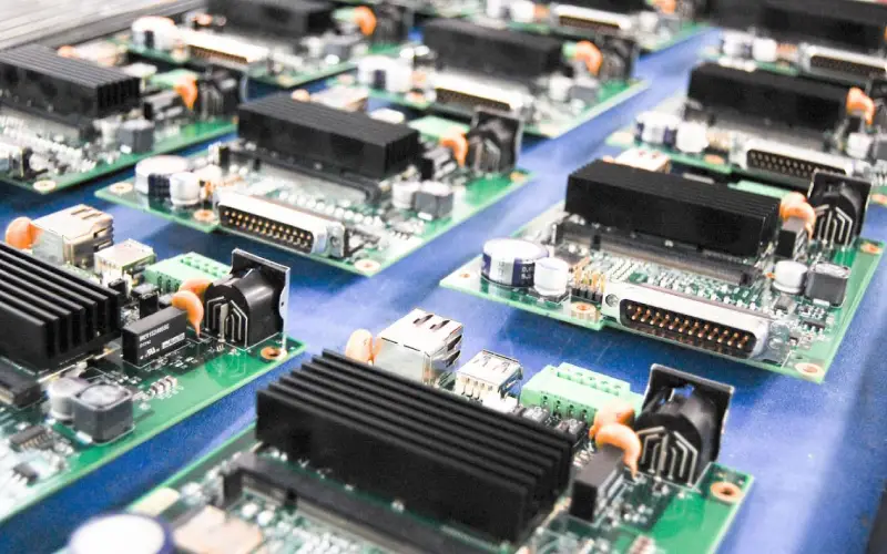
The final stage of the PCB Assembly Process is packaging and shipment.
Finished PCB assemblies should be protected against:
- Electrostatic discharge (ESD)
- Moisture
- Mechanical impact
- Dust
- Contamination
- Transportation vibration
ESD-safe bags, protective foam, dividers, and suitable shipping cartons can be used according to the product requirements.
For moisture-sensitive components and assemblies, appropriate moisture-control procedures should also be followed.
Before shipment, production and quality records should be reviewed to confirm that the order meets the customer’s specifications.
PCB Assembly Process Quality Control Flow
A typical professional production workflow can be summarized as:
Engineering Review → BOM Verification → PCB Fabrication → Component Procurement → SMT Assembly → SPI → Reflow Soldering → AOI → THT Assembly → Wave/Selective Soldering → X-Ray → ICT/FCT → Final Inspection → Labeling → ESD Packaging → Delivery
This structured approach helps manufacturers control quality from the initial design files through final product delivery.
Why Choose a Professional PCB Assembly Manufacturer?
Choosing the right manufacturing partner is important for both prototype development and production.
A capable PCB assembly manufacturer should provide:
- Engineering and DFM/DFA support
- PCB fabrication
- Component sourcing
- SMT assembly
- Through-hole assembly
- Mixed-technology assembly
- Automated inspection
- X-Ray inspection
- Electrical testing
- Functional testing
- Traceability
- ESD-safe packaging
- Prototype and production support
GoPCBA provides integrated PCB manufacturing and assembly services, including PCB fabrication, component procurement, SMT/THT assembly, PCBA testing, and box-build manufacturing.
For customers developing a new electronic product, Prototype PCB Assembly can help move a design from prototype to production while reducing development risk and improving manufacturing readiness.
For customers who want a single supplier to manage PCB fabrication, components, assembly, and related manufacturing operations, Turnkey PCB Assembly provides an integrated approach covering PCB fabrication, SMT, BGA, through-hole assembly, component sourcing, engineering support, inspection, programming, coating, and packaging.
Conclusion
The PCB Assembly Process is a comprehensive manufacturing workflow involving engineering review, material preparation, SMT assembly, through-hole assembly, inspection, testing, quality control, labeling, and packaging.
Each stage contributes to the reliability and performance of the finished PCBA. Proper BOM verification and DFA review reduce engineering risks, controlled SMT and THT processes improve assembly consistency, while AOI, X-Ray, ICT, and functional testing help identify defects before shipment.
By combining engineering expertise, advanced production equipment, reliable component sourcing, rigorous inspection, and flexible manufacturing capabilities, GoPCBA provides a one-stop solution for PCB fabrication and PCBA manufacturing from prototype development through production.
For your next PCB assembly project, Contact GoPCBA to discuss your Gerber files, BOM, Pick-and-Place data, assembly requirements, testing specifications, and production requirements.