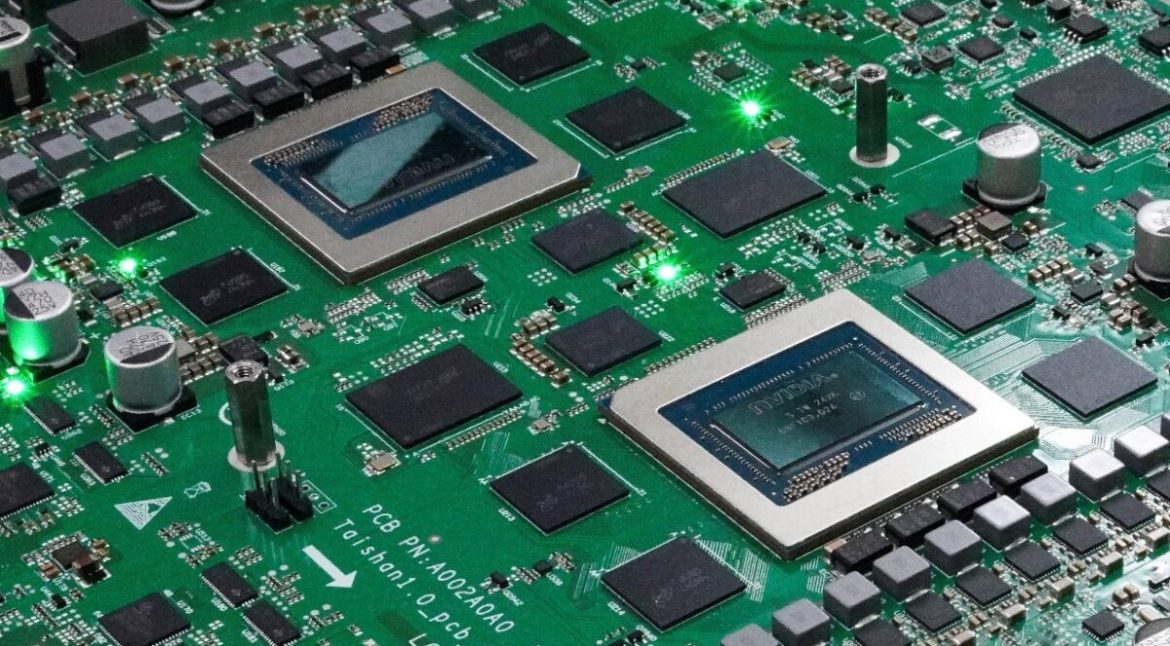
Multilayer Rigid-Flex PCB
A Multilayer Rigid-Flex PCB combines rigid circuit sections with flexible circuit sections in one integrated printed circuit board. By combining the mechanical stability of rigid materials with the flexibility of polyimide-based circuits, this technology enables compact three-dimensional electronic designs while reducing the need for cables, connectors, and separate circuit boards.
Unlike conventional rigid PCBs, rigid-flex structures can bend, fold, or conform to a product’s mechanical geometry. This makes them particularly useful when electronics must fit into limited spaces or operate under vibration, movement, or demanding environmental conditions.
Modern rigid-flex boards can incorporate multiple conductive layers, blind vias, buried vias, microvias, controlled-impedance structures, and high-density routing. These features make them suitable for advanced applications in medical electronics, aerospace, automotive electronics, industrial equipment, telecommunications, consumer electronics, and other high-reliability systems.
For projects requiring complex multilayer structures, manufacturers should evaluate the complete stack-up, material system, bend requirements, electrical performance, and assembly process before production. A professional PCB Manufacturing partner can help identify manufacturability risks at an early stage.
How Does a Rigid-Flex PCB Work?
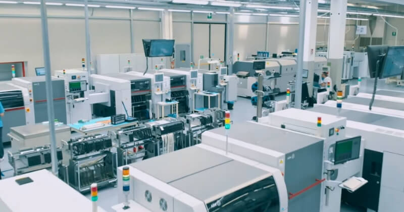
A rigid-flex PCB integrates rigid and flexible sections into a single circuit structure. The rigid portions provide mechanical support for components, connectors, and mounting points, while the flexible portions provide electrical connections between different rigid sections.
Flexible sections commonly use polyimide dielectric materials combined with copper conductors and protective coverlay. Rigid areas may use FR-4 or other suitable rigid laminate materials. Depending on the design, adhesive layers, bonding films, stiffeners, and reinforcement structures can also be incorporated.
In a multilayer construction, several copper layers are interconnected through plated through-holes, blind vias, buried vias, or microvias. This creates a three-dimensional interconnection architecture that can significantly reduce the need for external wiring.
The result is a circuit that can occupy complex mechanical spaces while maintaining electrical connectivity between fixed and moving sections.
For high-density designs, engineers may also integrate controlled impedance and advanced via structures. Current PCB manufacturing capabilities can support technologies such as HDI, microvias, blind and buried vias, controlled impedance, and rigid-flex construction.
Types of Rigid-Flex Circuit Boards
Rigid-flex PCBs can be classified according to their construction, number of layers, and application requirements.
Rigid-Flex Composite PCB
A rigid-flex composite PCB combines rigid and flexible sections within a single integrated structure. The design can use different interconnection structures, including blind and buried vias, to achieve high circuit density.
This configuration is suitable for products that require both mechanical support and flexible electrical connections while maintaining a compact overall form factor.
Rigid-Flex PCB
In a conventional rigid-flex construction, rigid and flexible sections are integrated through a controlled lamination process. The flexible areas provide bending capability, while the rigid areas support components and mechanical mounting.
Depending on the application, rigid-flex PCBs may be designed as single-sided, double-sided, multilayer, or HDI structures. Modern manufacturing services also support multilayer rigid-flex fabrication and assembly for demanding applications.
Key Design Considerations for Multilayer Rigid-Flex PCBs
Designing a reliable Rigid-Flex PCB Design requires both electrical and mechanical considerations. A rigid-flex circuit should not simply be treated as a rigid PCB with a thinner section. The materials, copper geometry, layer arrangement, bend radius, transition area, and assembly requirements all influence reliability.
Layer Stack-Up
The layer stack-up is one of the most important elements of a multilayer rigid-flex design.
Engineers need to define:
- Number of rigid and flexible layers
- Copper thickness
- Dielectric thickness
- Polyimide and rigid laminate materials
- Adhesive or bonding structures
- Coverlay construction
- Stiffener requirements
- Controlled-impedance structures
- Via and microvia configurations
The rigid and flexible sections must be mechanically and electrically balanced. Excessive layer count or copper thickness in a flexible region can increase stiffness and make bending more difficult.
For complex boards, early stack-up analysis can help optimize manufacturability, impedance performance, mechanical flexibility, and production yield. Professional PCB Design & Layout services can support stack-up design, impedance calculation, EMC considerations, and manufacturability optimization.
Bend Radius
Bend radius is critical to the long-term reliability of a flexible circuit.
A bend radius that is too small can place excessive mechanical stress on copper conductors and dielectric materials. Repeated bending can eventually lead to copper fatigue, cracking, delamination, or electrical failure.
The appropriate bend radius depends on factors such as:
- Number of flexible layers
- Copper thickness
- Copper type
- Static or dynamic bending
- Flexible dielectric thickness
- Coverlay construction
- Mechanical environment
Dynamic applications generally require more conservative mechanical design than applications involving only one-time forming.
Rigid-to-Flex Transition
The transition between rigid and flexible sections is a critical mechanical area.
Abrupt changes in thickness or copper density can concentrate mechanical stress. Designers should avoid sharp corners and unnecessary copper accumulation near the transition zone.
A gradual transition can help distribute stress and improve long-term reliability. The design should also prevent components, vias, or other rigid structures from interfering with the intended flexing area.
Component Placement
Components should generally be placed on rigid sections rather than in areas intended to bend.
Flexible areas need sufficient clearance to move without stressing solder joints, component bodies, or connectors. Components placed too close to a rigid-to-flex transition can create localized mechanical stress.
For assembled rigid-flex products, the assembly process should also be considered during the PCB design stage. Fixtures and handling methods may be required to prevent excessive bending during component placement and soldering.
Trace Routing
Trace routing directly affects flexible-section reliability.
Where possible, conductors should follow the intended bending direction and avoid unnecessary sharp corners. Trace geometry should be optimized to reduce stress concentration.
Engineers should also consider:
- Trace width
- Copper thickness
- Trace spacing
- Copper distribution
- Differential-pair routing
- Ground structures
- Impedance control
- Bend direction
- Transition geometry
For high-speed applications, electrical design and mechanical design must be evaluated together. Signal integrity, return paths, impedance, and electromagnetic compatibility can become increasingly important as circuit density and operating frequency increase.
Multilayer Rigid-Flex PCB Manufacturing Process
Reliable Rigid-Flex PCB Manufacturing requires precise control of multiple materials and processes. Unlike a conventional rigid board, rigid-flex fabrication must account for both electrical performance and mechanical flexibility.
1. Material Preparation
The manufacturing process begins with the selection and preparation of copper foil, polyimide materials, rigid laminates, coverlay, bonding materials, stiffeners, and other required materials.
Material selection should match the electrical, thermal, mechanical, and environmental requirements of the final application.
2. Flexible Core Fabrication
The flexible core is typically manufactured using a flexible dielectric material such as polyimide combined with copper foil.
The copper is patterned through imaging and etching processes to create the required circuit traces. Coverlay or other protective structures can then be applied to protect the flexible conductors.
3. Circuit Imaging and Etching
Photoimaging processes transfer the circuit pattern onto the copper surface. The unwanted copper is removed during etching, leaving the required conductor geometry.
Precise registration is important for multilayer rigid-flex boards because small dimensional variations can affect alignment between multiple layers.
4. Drilling
Mechanical drilling and laser drilling can be used according to the required hole and via structures.
Drilling may be required for:
- Through-holes
- Vias
- Blind vias
- Buried vias
- Microvias
- Component holes
Hole quality, registration accuracy, aspect ratio, and debris control must be carefully managed.
5. Copper Plating
After drilling, copper plating establishes electrical connections between conductive layers.
For multilayer boards, consistent plating coverage and copper thickness are essential for electrical reliability and long-term mechanical performance.
6. Rigid Section Lamination
Rigid sections are typically constructed from rigid laminate and prepreg materials. These structures are laminated together according to the defined stack-up.
Temperature, pressure, registration, and lamination time must be controlled to achieve stable bonding between the different material systems.
7. Integration of Rigid and Flexible Sections
The rigid and flexible structures are integrated through carefully controlled bonding and lamination processes.
This stage is especially important because the finished board must maintain both mechanical flexibility in designated areas and structural stability in rigid regions.
8. Surface Finishing and Final Processing
Depending on the application, surface finishes such as ENIG, HASL, OSP, immersion silver, immersion tin, ENEPIG, or gold plating may be used.
The final process can also include solder mask, silkscreen, stiffeners, coverlay processing, routing, laser cutting, and other application-specific operations.
Rigid-Flex PCB Assembly
After fabrication, rigid-flex boards can undergo SMT, through-hole, or mixed-technology assembly depending on the product architecture.
A typical assembly process may include:
- Solder paste printing
- Solder paste inspection
- Component placement
- Reflow soldering
- Through-hole insertion
- Selective or wave soldering
- AOI inspection
- X-Ray inspection
- Electrical testing
- Functional testing
The flexible sections require special handling because excessive mechanical force during assembly can damage the circuit.
Professional Flex and Rigid-Flex PCB Assembly services can integrate flexible and rigid-flex fabrication with SMT and other assembly processes.
For projects requiring both PCB fabrication and complete component assembly, PCB Assembly Services can provide a broader manufacturing workflow covering rigid, flexible, rigid-flex, multilayer, HDI, and other PCB technologies.
Quality Testing for Multilayer Rigid-Flex PCBs
Quality control is particularly important for rigid-flex boards because multiple materials, mechanical structures, and manufacturing processes are combined into one product.
Typical inspection and testing may include:
- Material verification
- Stack-up verification
- Dimensional inspection
- Copper thickness inspection
- Hole and via inspection
- AOI inspection
- X-Ray inspection
- Electrical testing
- Impedance testing
- Solderability inspection
- Assembly inspection
- Functional testing
- Final visual inspection
A complete Quality Management system can help control material verification, DFM review, production processes, electrical testing, component inspection, and final quality assurance.
Electrical testing is particularly important for multilayer structures because hidden interconnections cannot always be verified through visual inspection alone. Current PCB manufacturing processes can include AOI, X-Ray inspection, and 100% electrical testing according to board requirements.
Advantages of Multilayer Rigid-Flex PCBs
Higher Circuit Density
Multiple conductive layers allow more circuits to be integrated into a smaller physical area. This is valuable for compact electronic products with limited internal space.
Reduced Connectors and Wiring
A rigid-flex design can replace multiple cables, connectors, and separate circuit boards with one integrated PCB structure.
Fewer interconnections can simplify the electrical architecture and reduce potential mechanical or electrical failure points.
Three-Dimensional Installation
The flexible sections can be bent or folded to follow complex mechanical geometries. This enables designers to use available internal space more efficiently.
Lower Weight and Smaller Size
By reducing cables, connectors, and separate PCB assemblies, rigid-flex technology can contribute to a lighter and more compact electronic system.
Improved Reliability
A properly designed rigid-flex structure can reduce the number of connection points and improve resistance to vibration and mechanical movement.
However, reliability depends strongly on correct material selection, bend-radius design, transition geometry, manufacturing control, and application-specific testing.
Better Thermal and Mechanical Integration
The rigid sections provide stable mounting areas, while flexible sections can route signals around mechanical obstacles. This can simplify system architecture and improve overall integration.
Applications of Multilayer Rigid-Flex PCBs
Multilayer Rigid-Flex PCB technology is used across a wide range of advanced electronic products.
Medical Electronics
Medical equipment often requires compact and reliable electronic assemblies. Rigid-flex boards can be used in monitoring equipment, diagnostic systems, imaging equipment, wearable devices, and other medical electronics.
Aerospace and Defense
Aerospace electronics require lightweight construction, compact packaging, vibration resistance, and high reliability. Rigid-flex circuits can help reduce wiring while supporting complex three-dimensional electronic structures.
Automotive Electronics
Automotive systems increasingly require compact electronics capable of operating under vibration, temperature variation, and space constraints. Rigid-flex circuits can be used in control systems, sensors, cameras, infotainment equipment, and other automotive electronics.
Industrial Automation
Industrial machinery, robotics, motion-control equipment, instrumentation, and automation systems can benefit from flexible interconnections between fixed and moving sections.
For industrial applications, rigid, flexible, and rigid-flex boards can be selected according to the mechanical and electrical requirements of the equipment.
Telecommunications
High-density rigid-flex structures can support communication equipment where space, signal integrity, and interconnection reliability are important.
Consumer Electronics
Smartphones, wearable devices, cameras, portable electronics, headphones, and other compact products can use rigid-flex circuits to fit electronics into complex internal geometries.
Multilayer Rigid-Flex PCB Prototyping and Production
For new electronic products, it is often beneficial to validate the rigid-flex construction through prototype production before moving into larger-volume manufacturing.
Prototype evaluation can verify:
- Mechanical fit
- Bend performance
- Layer registration
- Component placement
- Electrical continuity
- Signal integrity
- Thermal performance
- Assembly compatibility
- Functional performance
For early-stage projects, Rapid PCBA Prototyping can support rigid, flex, and rigid-flex PCB prototypes, SMT and through-hole assembly, component procurement, and electrical or functional testing.
For smaller production quantities, Low Volume PCB Assembly can also be considered when a project requires pilot production, engineering validation, or initial market quantities.
How to Choose a Rigid-Flex PCB Manufacturer
Selecting the right manufacturing partner is critical for complex rigid-flex projects.
Before production, evaluate whether the manufacturer can support:
- Multilayer rigid-flex fabrication
- Flexible PCB materials
- Advanced drilling and plating
- Controlled impedance
- HDI and microvia technology
- DFM and DFA analysis
- Prototype production
- SMT and THT assembly
- Electrical testing
- AOI and X-Ray inspection
- Material traceability
- Production documentation
- Volume manufacturing
The supplier should also understand the interaction between mechanical bending requirements and electrical design requirements.
A manufacturer capable of integrating PCB fabrication, component sourcing, assembly, testing, and engineering support can simplify project management and reduce communication risks between multiple suppliers.
Conclusion
A Multilayer Rigid-Flex PCB provides an effective solution when an electronic product requires high circuit density, mechanical flexibility, compact packaging, and reliable electrical interconnection.
By combining rigid sections with flexible circuits, designers can reduce cables and connectors while creating three-dimensional electronic structures that fit demanding mechanical environments.
Successful rigid-flex products depend on careful Rigid-Flex PCB Design, appropriate materials, optimized layer stack-up, sufficient bend radius, controlled rigid-to-flex transitions, reliable manufacturing, and comprehensive testing.
From prototype development to production assembly, working with an experienced manufacturing partner can help identify design risks early and improve product reliability, manufacturability, and time to market.
For a rigid-flex PCB project, prepare your Gerber files, stack-up information, mechanical drawings, BOM, bend requirements, impedance specifications, and other technical requirements for engineering review before production.