What Is a Power Amplifier PCB?
A Power Amplifier PCB is a specialized printed circuit board designed to increase the power level of an electrical or electronic signal so it can effectively drive a load such as a loudspeaker, RF transmitter, motor, or other high-power electronic device.
Unlike a conventional PCB used primarily for signal processing and control, a power amplifier circuit board must handle higher currents, elevated voltages, thermal loads, and potentially high-frequency signals. The PCB therefore becomes an important part of the amplifier’s overall electrical, thermal, and mechanical design.
For demanding amplifier applications, the PCB must provide reliable current paths, appropriate grounding, sufficient thermal dissipation, and stable signal transmission. Depending on the application, the board may also require controlled impedance, heavy copper construction, multilayer routing, or specialized PCB materials.
For projects that require a complete manufacturing solution, PCB Manufacturing Services can integrate PCB fabrication with engineering and production requirements.
Why Is a Power Amplifier PCB Important?
Signal Amplification
The primary function of a power amplifier PCB is to support the amplification of relatively low-power electrical signals into signals capable of driving higher-power loads.
This capability is essential in audio equipment, wireless communication systems, industrial electronics, automotive electronics, and many other applications. The PCB must maintain stable electrical characteristics while carrying the current required by the amplifier’s output stage.
A well-designed board helps minimize unwanted losses, noise, parasitic effects, and signal distortion while supporting consistent amplifier performance.
Supporting Long-Distance Communication
Power amplifiers are widely used in telecommunications and RF systems because transmitted signals often require additional power before being sent through an antenna.
In these applications, PCB layout becomes especially important. Signal paths, grounding, impedance matching, component placement, and electromagnetic compatibility must be carefully controlled to maintain RF performance.
For complex RF and high-speed projects, professional PCB Design and Layout Services can help optimize stack-up, routing, impedance, EMC, and manufacturability before fabrication.
Improving Audio System Performance
Power amplifier PCBs are fundamental to audio equipment ranging from compact speakers and home audio systems to professional sound reinforcement equipment.
The board carries the audio signal through amplification stages and ultimately provides sufficient power to drive the speaker load. A carefully engineered PCB can help reduce unwanted noise, maintain signal integrity, and provide reliable operation under continuous load.
For high-power audio applications, the PCB must also accommodate the thermal and current requirements of the output devices.
Key Components of a Power Amplifier PCB
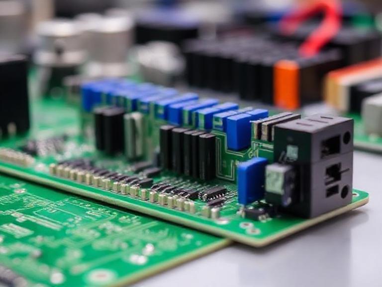
A typical power amplifier circuit board contains multiple active and passive components. Each component contributes to signal amplification, filtering, power regulation, protection, or thermal performance.
Transistors and Power Devices
Transistors are the primary active devices used in many amplifier circuits. Depending on the architecture, the design may use BJTs, MOSFETs, or other semiconductor devices.
Power transistors must be selected according to voltage rating, current capability, switching frequency, gain characteristics, efficiency, and thermal requirements.
Capacitors
Capacitors store electrical energy and help stabilize power rails, filter unwanted noise, couple or decouple signals, and support amplifier stability.
Power amplifier designs may require both large-value capacitors for bulk energy storage and smaller high-frequency capacitors for local decoupling.
Resistors
Resistors establish bias conditions, control current, create feedback networks, set gain, and provide protection or load functions.
Their resistance value, power rating, tolerance, and temperature coefficient should be selected according to the electrical requirements of the amplifier.
Inductors
Inductors are commonly used in filtering, power conversion, RF matching networks, and output filtering applications.
Their characteristics can directly influence amplifier efficiency, frequency response, and electromagnetic performance.
Heat Sinks and Thermal Interfaces
Power devices can generate significant heat during operation. Heat sinks, thermal pads, thermal vias, copper planes, and other thermal structures may therefore be necessary.
The PCB should be designed so that heat can efficiently move away from high-power components and into the appropriate cooling structure.
Key Design Considerations for a Power Amplifier PCB
Designing a reliable Power Amplifier PCB requires more than simply placing the schematic components onto a circuit board. Electrical, thermal, mechanical, and manufacturing requirements must be considered together.
Thermal Management
Heat Dissipation
Power amplifiers can generate substantial heat, especially when operating at high output power or under continuous load.
An effective thermal strategy may include:
- Large copper areas
- Thermal vias
- Heat sinks
- Thermal interface materials
- Metal-core or specialized PCB structures where appropriate
- Forced-air cooling
- Optimized component placement
Power devices should be positioned so that heat can be transferred efficiently to the intended cooling structure.
Thermal Layout
Thermal performance should be considered during PCB layout rather than after the board has been manufactured.
High-power components should have sufficient copper area and appropriate thermal connections. Thermal vias can also help transfer heat from component pads to internal or opposite-side copper structures.
For high-current electronics, Heavy Copper PCB Manufacturing can be considered when conventional copper thickness cannot provide the required current-carrying capacity or thermal performance.
Impedance Matching
Matching Networks
Impedance matching is particularly important in RF power amplifiers and other high-frequency applications.
A matching network may use inductors, capacitors, transmission lines, or combinations of these components to match the amplifier output to the intended load.
Proper matching can improve power transfer and efficiency while reducing unwanted reflections.
Simulation and Modeling
Circuit simulation and electromagnetic modeling can help engineers evaluate impedance behavior over the intended frequency range.
This is particularly useful when designing high-frequency amplifier PCBs, where parasitic capacitance, inductance, trace geometry, dielectric properties, and component placement can significantly influence performance.
PCB Layout Considerations
Minimize Signal Path Length
Short and controlled signal paths can help reduce parasitic effects, unwanted coupling, and signal degradation.
This becomes increasingly important as operating frequency increases. High-current loops should also be kept compact to reduce electromagnetic radiation and switching noise.
Separate Power and Sensitive Signal Areas
The power section and sensitive signal-processing circuits should be appropriately separated.
Careful zoning can reduce unwanted coupling between high-current switching circuits and low-level audio, control, or feedback signals.
A solid grounding strategy and appropriate power distribution can further improve system stability.
Ground and Power Planes
Ground planes provide low-impedance return paths and can help reduce noise and electromagnetic interference.
Power planes or large copper regions can distribute current more effectively and reduce voltage drops across the board.
For high-speed or RF amplifier designs, the stack-up and return-current path should be considered together with controlled-impedance routing.
Component Selection for Power Amplifier PCBs
Power Handling Capability
Every major component must be selected according to the amplifier’s electrical operating conditions.
Important parameters include:
- Maximum voltage
- Continuous and peak current
- Power dissipation
- Operating temperature
- Frequency range
- Component derating
- Expected service life
Power components should have adequate safety margins rather than being operated continuously at their absolute maximum ratings.
Frequency Response
Component characteristics can change with frequency.
For RF and high-frequency amplifier designs, designers must consider parasitic capacitance, equivalent series resistance, equivalent series inductance, package characteristics, and PCB geometry.
For audio amplifiers, component selection should also support the required frequency response, distortion characteristics, stability, and noise performance.
PCB Materials and Construction
The PCB material and construction should be selected according to the amplifier’s electrical, thermal, mechanical, and environmental requirements.
Common considerations include:
- Number of PCB layers
- Copper thickness
- Dielectric thickness
- Board thickness
- Surface finish
- Thermal performance
- Controlled impedance
- Operating frequency
- Mechanical dimensions
For conventional amplifier electronics, standard FR-4 materials may be suitable. More demanding RF or thermal applications may require specialized materials or construction techniques.
Modern PCB manufacturing can also support multilayer, high-frequency, rigid-flex, HDI, controlled-impedance, and heavy-copper structures depending on project requirements.
Prototype Development and Testing
Iterative Prototyping
A reliable amplifier design often requires multiple prototype iterations.
Prototype testing allows engineers to evaluate:
- Output power
- Frequency response
- Gain
- Total harmonic distortion
- Noise
- Efficiency
- Thermal performance
- Electromagnetic compatibility
- Load stability
Problems discovered during prototype testing can then be addressed through circuit, component, PCB layout, or thermal design modifications.
Electrical and Functional Testing
Comprehensive testing should be performed under representative operating conditions.
Depending on the product, testing may include electrical inspection, functional testing, load testing, temperature testing, aging tests, and other customer-specific validation requirements.
A professional PCBA Assembly Service can combine SMT, through-hole assembly, inspection, and testing processes to support the transition from prototype to production.
Reliability and Quality Requirements
EMI and EMC Considerations
Power amplifiers can generate significant electromagnetic energy, particularly when high-current or high-frequency switching devices are involved.
Poor grounding, large current loops, long traces, impedance discontinuities, and inadequate filtering can contribute to EMI problems.
Good PCB design practices include:
- Maintaining controlled return-current paths
- Minimizing high-current loop areas
- Separating noisy and sensitive circuits
- Using appropriate filtering
- Controlling impedance where required
- Providing adequate shielding provisions
- Avoiding unnecessary trace lengths
EMI control is especially important when the amplifier is integrated into a larger electronic system.
Manufacturing Quality Control
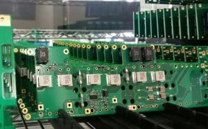
A reliable amplifier board depends not only on circuit design but also on consistent manufacturing.
Important manufacturing controls include:
- PCB specification verification
- Material verification
- Copper thickness control
- Solder mask inspection
- Component verification
- SMT process control
- AOI inspection
- X-ray inspection where appropriate
- Functional testing
- Final quality inspection
A structured PCB Quality Management Process helps ensure that manufacturing parameters, BOM information, PCB specifications, assembly processes, and testing requirements are controlled throughout production.
Applications of Power Amplifier PCBs
Power amplifier PCBs are used across a wide range of electronic products and systems.
Audio Equipment
Applications include:
- Home audio amplifiers
- Professional audio systems
- Powered speakers
- Public address systems
- Automotive audio systems
- Home theater equipment
Telecommunications
Power amplifier circuits are widely used in:
- Wireless communication equipment
- RF transmitters
- Cellular infrastructure
- Radio systems
- Satellite communication equipment
Automotive Electronics
Automotive amplifier PCBs can be used in audio systems, communication equipment, vehicle control electronics, and other applications requiring reliable signal or power amplification.
Automotive environments can introduce additional requirements related to temperature, vibration, electromagnetic compatibility, and long-term reliability.
Industrial Electronics
Industrial applications may include instrumentation, motor control, industrial communication, automation equipment, and specialized power electronics.
For industrial projects, PCB manufacturing and assembly must account for operating conditions, electrical loads, environmental requirements, and production reliability. GOPCBA also provides Industrial PCB Assembly solutions for industrial control applications.
How to Choose a Power Amplifier PCB Manufacturing Partner
Selecting the right manufacturing partner is important when the amplifier PCB has demanding electrical or thermal requirements.
Consider the manufacturer’s ability to support:
- PCB design review
- DFM and DFA analysis
- Multilayer PCB fabrication
- Controlled impedance
- Heavy copper PCB production
- SMT and THT assembly
- Component procurement
- Thermal management requirements
- Electrical testing
- Functional testing
- Prototype and volume production
An integrated manufacturing partner can reduce communication gaps between PCB fabrication, component sourcing, assembly, and testing.
For projects requiring engineering support and complete manufacturing coordination, Contact GOPCBA to discuss your PCB or PCBA requirements and provide your Gerber, BOM, drawings, or other production documentation.
Conclusion
A power amplifier PCB is much more than a platform for mounting electronic components. It is a critical part of the amplifier’s electrical, thermal, mechanical, and reliability architecture.
Successful Power Amplifier Circuit Board development requires careful attention to current capacity, thermal management, impedance matching, grounding, signal routing, component selection, EMI control, and manufacturability.
From prototype development through production, integrating PCB design, fabrication, assembly, inspection, and testing can significantly improve manufacturing consistency and reduce development risk.
With the right engineering and manufacturing strategy, a properly designed Power Amplifier PCB can provide stable signal amplification, efficient power delivery, reliable thermal performance, and long-term operational stability across audio, RF, automotive, telecommunications, and industrial applications.