Laser Sensing PCB: Transforming Precision and Efficiency
Integrating laser sensing technology into printed circuit boards has opened new possibilities for modern electronic systems. A Laser Sensing PCB combines a laser sensor with the electrical circuitry required for signal processing, power management, communication, and control. This integrated approach enables accurate detection, distance measurement, positioning, and motion analysis in compact electronic products.
Today, Laser Sensing Technology is increasingly used in industrial automation, automotive electronics, consumer electronics, medical equipment, robotics, and other applications where fast and precise measurement is essential.
For projects that require customized circuit board fabrication, explore our PCB Manufacturing capabilities for prototype and production requirements.
What Is a Laser Sensing PCB?
A Laser Sensor PCB is a printed circuit board designed to integrate one or more laser-based sensing components with the electronic circuitry required to operate and process their signals.
Unlike conventional sensors that may rely on simple light or electrical detection, laser sensors use a focused optical beam to detect objects, determine distance, measure movement, or identify changes in position. Depending on the sensing principle, the PCB can receive optical information and convert it into digital or analog data for further processing.
A typical laser sensing circuit may include:
- Laser diode or laser emitter
- Photodetector or receiver
- Signal conditioning circuitry
- Microcontroller or processor
- Power management circuitry
- Communication interfaces
- Protection components
- Calibration and control circuits
The PCB therefore acts as the electronic foundation of the sensing system, providing electrical connectivity while supporting the mechanical and thermal requirements of the application.
For applications that require complete fabrication and assembly, PCB Assembly can integrate the required components onto the finished board.
How Does a Laser Sensor Work?
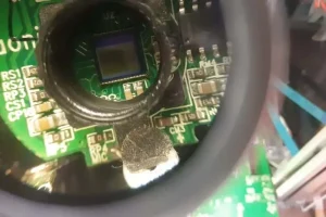
The operating principle of a Laser Sensor PCB depends on the type of laser sensing technology being used. In many systems, a laser emitter produces a narrow beam that is directed toward a target. The reflected or scattered light is then detected by a receiver.
The electronic circuit processes the received signal and calculates the required measurement.
For distance measurement, the system may determine how long it takes the laser pulse to travel to the target and return to the sensor. This principle is commonly known as Time of Flight, or ToF.
Other systems determine distance by analyzing the position or angle of the reflected laser beam, while Doppler-based systems analyze frequency changes associated with moving objects.
The basic sensing sequence can be summarized as:
1. Laser Emission
The laser diode generates a controlled optical beam and directs it toward the target.
2. Optical Reflection
The emitted laser light interacts with the target surface and part of the light returns toward the sensing receiver.
3. Signal Detection
A photodetector receives the reflected optical signal and converts it into an electrical signal.
4. Signal Processing
The PCB processes the electrical signal using analog circuitry, digital processing, or a microcontroller.
5. Measurement Output
The calculated distance, position, velocity, or detection result is transmitted to the main control system through an appropriate interface.
Benefits of Laser Sensing PCBs
A well-designed Laser Sensing PCB can provide several important advantages for modern electronic products.
High Measurement Precision
Laser sensing can provide highly accurate measurements, making it suitable for applications where conventional detection technologies may not provide sufficient resolution.
Precision is particularly important in industrial positioning, automated inspection, robotics, dimensional measurement, and advanced automotive systems.
Fast Response
Laser sensors can capture measurements at high speed, allowing electronic systems to monitor rapidly changing environments and respond in real time.
This capability is valuable for automated production lines, motion control, object detection, and dynamic measurement systems.
Compact Integration
Integrating the sensor and supporting electronics onto a PCB can reduce the overall system footprint. This makes laser sensing suitable for compact products where available installation space is limited.
For more advanced compact electronics, manufacturers can also combine laser sensing circuitry with HDI and multilayer PCB technologies.
Reliable Signal Processing
The PCB can place the laser sensor, signal-conditioning circuitry, processor, and communication interface within a controlled electronic architecture.
This can help reduce unnecessary wiring and improve signal integrity when the layout is properly designed.
Flexible System Integration
Laser sensing circuits can be customized for different measurement ranges, communication interfaces, power requirements, and mechanical configurations.
This flexibility allows the same basic sensing concept to be adapted for industrial, automotive, medical, consumer, and robotic applications.
Types of Laser Sensing PCBs
Different sensing principles require different electronic and optical architectures. The most common types include ToF, laser triangulation, and laser Doppler systems.
ToF Sensor PCB
A ToF Sensor PCB measures the time required for a laser signal to travel to an object and return to the receiver.
The measured travel time can then be converted into distance information. ToF technology is widely used in distance measurement, object detection, depth sensing, robotics, and automotive electronics.
The PCB must provide accurate timing, signal processing, power regulation, and communication functions to ensure reliable measurement performance.
Laser Triangulation Sensor PCB
Laser triangulation determines distance by analyzing the position or angle of reflected laser light.
The laser projects a beam onto the target, while an optical receiver detects the reflected light at a specific position. Based on the geometry of the optical system, the electronics can calculate the distance to the target.
This approach is particularly useful for high-precision industrial measurement, surface inspection, dimensional control, and automated quality inspection.
Laser Doppler Sensor PCB
Laser Doppler sensing is designed to detect movement and velocity by analyzing changes in the frequency of reflected laser light.
These systems can be used for non-contact velocity measurement and motion analysis. The PCB requires appropriate high-speed signal-processing circuitry to extract useful information from the optical signal.
Applications of Laser Sensing PCBs
The accuracy, speed, and compact integration offered by Laser Sensor Applications make this technology suitable for a broad range of industries.
Industrial Automation
In industrial automation, laser sensors can be used for:
- Object detection
- Position measurement
- Dimensional inspection
- Machine alignment
- Robot positioning
- Automated quality control
- Distance measurement
Laser sensing allows machines to obtain precise information without physical contact with the target.
For industrial electronic systems requiring customized circuit boards and assembly, our Industrial PCB Assembly solutions support a wide range of rigid, flexible, and rigid-flex PCB requirements.
Automotive Electronics
Automotive systems increasingly rely on sensors for object detection, distance measurement, positioning, and advanced driver-assistance functions.
Laser-based sensing can support applications such as:
- Object detection
- Distance measurement
- Parking assistance
- Vehicle positioning
- Advanced driver-assistance systems
- Robotics and autonomous mobility systems
Automotive applications typically require careful consideration of temperature, vibration, electromagnetic compatibility, reliability, and long-term operating stability.
Consumer Electronics
Compact laser sensing modules can be incorporated into smartphones, cameras, smart devices, robotics products, and other consumer electronics.
Typical applications include:
- Autofocus
- Depth measurement
- Gesture detection
- Object detection
- Distance measurement
- 3D sensing
The small form factor of PCB-based laser sensing electronics is particularly useful where internal space is limited.
Medical and Healthcare Equipment
Medical equipment often requires accurate and repeatable measurements. Laser sensing can be incorporated into specialized monitoring, diagnostic, positioning, and measurement equipment.
The PCB design must be developed according to the electrical, environmental, reliability, and regulatory requirements of the specific medical application.
Robotics
Robotic systems require accurate information about their surrounding environment to navigate, position components, and interact with objects.
Laser sensors can provide distance and position information for:
- Autonomous navigation
- Robotic arms
- Object detection
- Collision avoidance
- Automated inspection
- Warehouse robots
How to Choose the Right Laser Sensor for a PCB
Selecting the appropriate laser sensor requires more than simply choosing a component with the desired measurement range. The sensor, PCB, optical system, firmware, and mechanical structure must work together as a complete system.
Important considerations include:
Measurement Range
Determine the minimum and maximum distance that the system needs to measure. The selected sensor should provide sufficient range while maintaining the required accuracy.
Measurement Accuracy
Define the required resolution, repeatability, and measurement tolerance before selecting the sensor and PCB architecture.
Operating Environment
Temperature, humidity, dust, vibration, ambient light, and other environmental conditions can affect sensing performance.
The PCB material, component selection, enclosure, and thermal design should therefore match the intended operating environment.
Power Consumption
Battery-powered and portable products often require extremely efficient power management. The laser emitter, receiver, processor, and supporting circuits should be evaluated as a complete power budget.
PCB Size and Layer Structure
The available installation space determines the appropriate board dimensions, layer count, component placement, and routing strategy.
High-density designs may benefit from advanced PCB technologies such as HDI, microvias, controlled impedance, and multilayer construction.
Signal Integrity
Laser sensors can generate sensitive analog and high-speed signals. PCB routing should separate sensitive signal paths from noisy power or digital circuits where necessary.
Grounding, shielding, return paths, power integrity, and component placement should all be considered during PCB layout.
Thermal Management
Laser diodes, processors, regulators, and other active components generate heat. Excessive temperature can affect both electronic reliability and optical measurement accuracy.
Thermal management should therefore be incorporated into the PCB design from the beginning.
Laser Sensing PCB Manufacturing Considerations
A reliable Laser Sensor PCB requires careful manufacturing control because optical sensing electronics may contain sensitive analog, digital, and high-frequency circuits.
Important manufacturing considerations include:
- Controlled PCB layer stack-up
- Accurate component placement
- Stable dielectric materials
- Controlled impedance when required
- Reliable solder joints
- Precise drilling and registration
- Appropriate surface finish
- Electrical testing
- AOI inspection
- Functional testing
- Thermal and environmental validation
For projects that require both PCB fabrication and component assembly, Rapid PCBA Prototyping can help accelerate the transition from an engineering design to functional prototypes.
Laser Sensing PCB Assembly
After PCB fabrication, the laser sensing board may require SMT, through-hole, or mixed-technology assembly.
The assembly process can include:
- Solder paste printing
- SPI inspection
- Component placement
- Reflow soldering
- AOI inspection
- Through-hole assembly when required
- X-ray inspection for selected components
- Electrical testing
- Firmware programming
- Functional testing
Component placement is particularly important for laser sensing systems because the physical relationship between the laser emitter, optical receiver, and mechanical structure can directly affect measurement performance.
For more demanding projects, PCBA Capabilities include support for different PCB structures, component packages, assembly technologies, inspection, and production requirements.
Quality Control for Laser Sensing PCBs
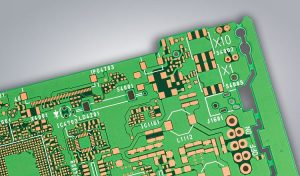
Quality control should cover both PCB manufacturing and the completed sensing assembly.
A comprehensive quality program may include:
- Incoming material inspection
- PCB dimensional inspection
- Layer and stack-up verification
- Copper thickness verification
- AOI inspection
- X-ray inspection
- Electrical testing
- Component verification
- Solder joint inspection
- Functional testing
- Optical performance verification
- Final inspection
For prototype and production projects, engineering review and Design for Manufacturing analysis can also help identify potential issues before production begins.
Why Choose a Professional PCB Manufacturing Partner?
Laser sensing electronics combine optical components, electronic circuits, mechanical structures, and software. As a result, the PCB manufacturer needs to understand more than basic circuit board fabrication.
A capable manufacturing partner should be able to support:
- PCB engineering review
- DFM and DFA analysis
- Rigid and flexible PCB fabrication
- Multilayer PCB manufacturing
- Component sourcing
- SMT and through-hole assembly
- Electrical testing
- Functional testing
- Prototype production
- Low-volume production
- Mass production
A single manufacturing partner can also simplify communication between PCB fabrication, component procurement, assembly, testing, and production engineering.
Conclusion
Laser Sensing PCB technology is helping manufacturers develop smaller, faster, and more accurate electronic sensing systems. By integrating laser emitters, receivers, signal-processing circuits, processors, and communication interfaces onto a carefully designed PCB, engineers can create compact sensing solutions for demanding applications.
From industrial automation and robotics to automotive electronics, consumer devices, and medical equipment, Laser Sensing Technology provides an effective method for non-contact measurement, object detection, positioning, and motion analysis.
The success of a laser sensing product depends on the complete system design—not only the sensor itself. PCB layout, material selection, signal integrity, thermal management, assembly accuracy, optical alignment, and functional testing should all be considered during product development.
With the right engineering and manufacturing partner, a laser sensing concept can be developed from prototype through production while maintaining the precision, reliability, and consistency required by modern electronic applications.
Frequently Asked Questions
What is a Laser Sensing PCB?
A Laser Sensing PCB is a printed circuit board designed to integrate laser sensing components with power management, signal processing, control, and communication circuits. It can be used to detect objects, measure distance, determine position, or analyze motion.
What is a Laser Sensor PCB used for?
A Laser Sensor PCB can be used for industrial automation, robotics, automotive electronics, consumer electronics, medical equipment, dimensional inspection, positioning, and other applications requiring accurate non-contact measurement.
What is a ToF Sensor PCB?
A ToF Sensor PCB integrates a Time-of-Flight sensing system with the supporting electronic circuitry needed to measure the travel time of a laser signal. The travel time can be used to calculate the distance between the sensor and an object.
What are the main types of laser sensors?
Common types include ToF sensors, laser triangulation sensors, and laser Doppler sensors. Each technology uses a different measurement principle and is suited to different applications.
What PCB technologies are suitable for laser sensing applications?
Depending on system complexity, laser sensing products may use single-layer, multilayer, HDI, flexible, rigid-flex, high-speed, or controlled-impedance PCB technologies. The appropriate structure depends on electrical, mechanical, optical, thermal, and space requirements.
What information is required to manufacture a Laser Sensing PCB?
Typical manufacturing documentation includes Gerber files or ODB++ data, drill files, PCB stack-up information, BOM, pick-and-place files, assembly drawings, component specifications, surface-finish requirements, and functional or testing requirements.