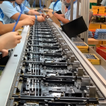
Step-Structure Rigid-Flex PCB
Modern electronic products continue to become smaller, lighter, and more integrated. Conventional rigid circuit boards can provide excellent mechanical stability, but they are difficult to fit into products with curved, folded, or three-dimensional structures. Flexible circuits solve many of these mechanical challenges, but they may not provide enough structural support for components and connectors.
A Step-Structure Rigid-Flex PCB combines rigid and flexible sections within a single circuit board structure. This approach provides mechanical support where components are mounted while allowing designated areas to bend, fold, or adapt to the internal geometry of the product.
For applications requiring compact packaging, reduced interconnections, and three-dimensional assembly, rigid-flex technology can provide an effective alternative to separate rigid PCBs, flexible cables, and connectors.
What Is a Step-Structure Rigid-Flex PCB?
A step-structure rigid-flex PCB is a specialized form of rigid-flex circuit in which the board profile changes between rigid and flexible sections. Instead of maintaining the same construction throughout the entire PCB, different areas are designed with different mechanical characteristics.
The rigid sections typically provide structural support for ICs, connectors, switches, BGA packages, and other components. The flexible sections use bendable materials and are designed to accommodate folding or controlled movement.
The transition between these areas is particularly important. A properly engineered step structure creates a controlled transition between rigid and flexible zones, helping distribute mechanical stress and supporting more compact three-dimensional packaging.
A typical construction may include:
- Rigid FR-4 or high-performance rigid materials
- Flexible polyimide-based layers
- Copper conductors
- Coverlay in flexible areas
- Bonding materials
- Plated through holes and microvias where required
- Stiffeners or localized reinforcement
- Controlled rigid-to-flex transition areas
For projects requiring more complex structures, Rigid-Flex PCB Manufacturing should be considered during the design stage rather than treated only as a fabrication requirement.
Step-Structure Rigid-Flex PCB Structure
A step-structure rigid-flex board can be divided into several functional regions.
Rigid Section
The rigid section provides mechanical support for electronic components. It is commonly constructed using FR-4 or other rigid PCB materials.
Components such as processors, connectors, memory devices, power components, and communication interfaces can be mounted on these areas.
The rigid section also helps maintain dimensional stability during assembly and operation.
Flexible Section
The flexible section is designed to bend or fold according to the mechanical requirements of the product. Polyimide is widely used because of its flexibility, thermal performance, and reliability.
The flexible area can route signals between two or more rigid sections without requiring separate cables or connectors.
This is particularly useful when the electronic assembly must conform to an enclosure or occupy a three-dimensional mechanical space.
Transition Zone
The transition zone connects the rigid and flexible portions of the circuit. It is one of the most important areas in a Rigid-Flex PCB Design.
Mechanical stress can concentrate around an improperly designed rigid-to-flex transition. Designers therefore need to consider copper distribution, layer construction, bend requirements, material compatibility, and mechanical reinforcement.
A controlled transition helps improve durability and reduces the risk of cracking, delamination, or conductor fatigue during bending and assembly.
Component Mounting Areas
Components are normally concentrated on rigid sections where the board provides adequate mechanical support.
Keeping heavy or mechanically stressed components away from active flexing areas can improve long-term reliability.
Signal and Power Routing
Electrical connections can pass continuously through rigid and flexible sections. This eliminates many cable-based interconnections and can simplify the overall product architecture.
However, signal integrity, impedance control, power distribution, and grounding must be considered across the complete rigid-flex stack-up.
Bend Radius Area
The flexible region must be designed around an appropriate minimum bend radius.
The actual allowable bend radius depends on the layer count, copper thickness, material construction, bending direction, and whether the application involves static folding or repeated dynamic movement.
For dynamic applications, the flex structure should be specifically designed and qualified for the expected number of bending cycles.
Simplified Step-Structure Rigid-Flex PCB Comparison
| Aspect | Description |
|---|---|
| Construction | Combination of rigid and flexible PCB sections within one circuit structure |
| Rigid materials | FR-4 and other rigid PCB materials |
| Flexible materials | Polyimide and other suitable flexible substrates |
| Main purpose | Balance structural stability with mechanical flexibility |
| Transition area | Controlled transition between rigid and flexible sections |
| Component placement | Components are primarily mounted on rigid areas |
| Interconnection | Flexible sections can replace cables and connectors |
| Mechanical support | Rigid areas provide support for components and interfaces |
| Manufacturing | Requires specialized lamination, drilling, routing, and process control |
| Testing | Electrical, dimensional, mechanical, and reliability testing may be required |
| Applications | Medical, automotive, aerospace, industrial, wearable, and compact electronics |
Types of Rigid-Flex PCBs
Rigid-flex circuits can be manufactured in several configurations depending on electrical, mechanical, and packaging requirements.
Single-Layer Flexible Rigid-Flex PCB
This construction uses a flexible circuit layer integrated with rigid sections. It can be suitable for relatively simple interconnection requirements and applications where controlled flexibility is needed.
Double-Sided Rigid-Flex PCB
Double-sided structures provide conductive patterns on both sides of the flexible region. This allows greater routing density and more complex electrical connections.
Multilayer Rigid-Flex PCB
A Multilayer Rigid-Flex PCB integrates multiple conductive layers with rigid and flexible sections.
Multilayer construction is useful for high-density electronics that require power planes, ground planes, multiple signal layers, controlled impedance, and compact routing.
HDI Rigid-Flex PCB
HDI rigid-flex technology can combine flexible mechanical integration with high-density interconnection techniques such as microvias and fine-pitch routing.
This configuration is especially useful for compact products where board area is highly constrained.
Dynamic Rigid-Flex PCB
Dynamic applications require the flexible section to withstand repeated movement. The material stack-up, copper geometry, bend radius, and flex-layer construction must be optimized for the expected operating cycle.
Custom Rigid-Flex PCB
Custom rigid-flex structures can be developed around the mechanical geometry, electrical architecture, component arrangement, and environmental requirements of a specific product.
For applications requiring complete PCB fabrication and production support, PCB Manufacturing can provide a broader manufacturing solution covering rigid, flexible, rigid-flex, HDI, and multilayer technologies.
Step-Structure Rigid-Flex PCB Cross-Section
The cross-section of a step-structure rigid-flex PCB depends on the required electrical and mechanical performance.
A typical structure may contain:
Rigid Area → Transition Area → Flexible Area → Transition Area → Rigid Area
The rigid sections may contain multiple FR-4-based layers, while the flexible section uses one or more flexible dielectric and copper layers.
The step configuration can also be used to control the thickness and mechanical profile of specific regions. This can make the PCB easier to integrate into compact housings where a uniform board thickness would create mechanical interference.
For complex multilayer constructions, the stack-up should be developed together with the PCB manufacturer. This allows material thickness, copper weight, via structures, impedance requirements, and lamination processes to be evaluated before fabrication.
Advantages of Step-Structure Rigid-Flex PCBs
Space Optimization
One of the primary benefits of rigid-flex technology is improved space utilization.
Rigid sections can accommodate densely populated electronic components, while flexible sections can fold around mechanical structures. This enables designers to create compact three-dimensional assemblies that would be difficult to achieve with conventional rigid boards and separate cables.
This is especially valuable in wearable electronics, medical equipment, automotive electronics, aerospace systems, and compact industrial devices.
Reduced Weight
A rigid-flex assembly can replace multiple rigid boards, wire harnesses, connectors, and flexible cables.
Reducing these additional components can lower overall system weight and simplify the mechanical structure.
Weight reduction is particularly important in aerospace, drones, automotive systems, portable electronics, and other applications where every gram matters.
Fewer Interconnections
Connectors and cables can become potential failure points in an electronic system.
A rigid-flex PCB can integrate electrical connections directly into the circuit structure, reducing the number of external cables and connectors.
This can simplify assembly while improving system integration and potentially increasing long-term reliability.
Improved Mechanical Reliability
Rigid sections provide mechanical support for components and connectors, while flexible sections accommodate controlled bending.
This combination allows the PCB to match the mechanical requirements of the product without sacrificing the structural support needed for component mounting.
Simplified Three-Dimensional Assembly
Rigid-flex circuits can be folded or positioned into three-dimensional configurations during final assembly.
This can simplify internal wiring and help engineers make better use of irregularly shaped product enclosures.
Better System Integration
Instead of treating the PCB, cable assembly, and connectors as separate components, rigid-flex technology can integrate several functions into one engineered circuit structure.
This can reduce assembly complexity and provide a cleaner overall product architecture.
For complete assembly requirements, Flex and Rigid-Flex PCB Assembly supports single-sided, double-sided, multilayer, HDI, and rigid-flex PCB assembly solutions.
Step-Structure Rigid-Flex PCB Design Considerations
Designing a reliable step-structure rigid-flex circuit requires careful coordination between electrical, mechanical, and manufacturing requirements.
Material Selection
Material selection directly affects flexibility, thermal performance, dielectric properties, and reliability.
Rigid areas may use standard FR-4, high-Tg materials, or application-specific materials. Flexible sections commonly use polyimide-based constructions.
The materials must also be compatible with the required lamination, plating, soldering, and assembly processes.
Stack-Up Design
Stack-up design is critical for electrical performance and mechanical reliability.
Engineers should evaluate:
- Number of rigid and flexible layers
- Copper thickness
- Dielectric thickness
- Controlled impedance requirements
- Ground and power planes
- Signal routing
- Via structures
- Flexible-section thickness
- Mechanical transition geometry
For high-speed applications, the rigid-flex stack-up must also support signal integrity and predictable impedance.
Bend Radius
The minimum bend radius should be defined before layout begins.
Sharp bends can place excessive mechanical stress on copper conductors and dielectric layers. Designers should avoid unnecessary sharp transitions and should ensure that traces, vias, and components are located appropriately relative to the flexing area.
Repeated bending requires stricter design controls than a one-time installation bend.
Copper Routing
Copper distribution can significantly influence the mechanical behavior of the flexible section.
Where appropriate, traces should be routed to reduce localized stress. Designers should also consider conductor geometry, layer symmetry, copper thickness, and the expected bending direction.
Via Placement
Vias should be carefully positioned around flexible areas. Depending on the construction, vias in highly active bending regions may create additional mechanical stress.
Manufacturing capabilities should therefore be considered when defining via structures and transition zones.
Connector Placement
Connectors are normally mounted on rigid sections because these areas provide greater mechanical support.
If a connector must interact directly with a flexible region, additional mechanical reinforcement may be required.
Thermal Management
High-power components should generally remain on rigid sections where thermal management is easier to implement.
The design should consider heat spreading, copper areas, thermal vias, component temperature, and the surrounding mechanical enclosure.
Applications of Step-Structure Rigid-Flex PCBs
Wearable Electronics
Wearable products require small dimensions, low weight, and mechanical adaptability.
Rigid-flex structures can connect sensors, processors, communication modules, batteries, and interfaces while conforming to the shape of the wearable enclosure.
Medical Electronics
Medical equipment often requires compact packaging and reliable electrical connections.
Rigid-flex circuits can be used in portable diagnostic equipment, monitoring systems, medical instruments, and other electronic devices where space and mechanical integration are important.
For broader electronics manufacturing requirements, PCB Assembly Services can integrate PCB fabrication, component sourcing, SMT, THT, inspection, testing, and final assembly.
Automotive Electronics
Automotive electronics must withstand vibration, thermal cycling, humidity, and long operating periods.
Rigid-flex circuits can support compact electronic modules, sensors, control systems, infotainment equipment, positioning systems, and other applications where conventional cable assemblies may be difficult to integrate.
Aerospace and Defense
Weight, reliability, and packaging efficiency are major considerations in aerospace and defense electronics.
Rigid-flex technology can reduce wiring and connector requirements while allowing electronics to fit into constrained three-dimensional spaces.
Industrial Electronics
Industrial equipment often requires reliable connections in environments involving vibration, temperature changes, and continuous operation.
Rigid-flex PCBs can simplify internal wiring and provide a compact solution for sensors, controllers, automation systems, and instrumentation.
Telecommunications and IoT
Compact communication modules and IoT devices frequently require high-density routing within limited mechanical spaces.
Rigid-flex and HDI technologies can help integrate multiple circuit functions while maintaining a compact form factor.
Manufacturing Challenges
Complex Fabrication
Rigid-flex fabrication is more complex than conventional rigid PCB manufacturing.
The manufacturer must coordinate material preparation, lamination, drilling, copper plating, imaging, routing, coverlay processing, and final inspection across different structural regions.
A capable manufacturing partner should evaluate the complete design before production to identify potential manufacturing risks.
Material Compatibility
Rigid and flexible materials have different mechanical and thermal characteristics.
Poor material selection or inappropriate process parameters can result in dimensional instability, delamination, cracking, or other reliability problems.
Transition Reliability
The rigid-to-flex transition is a critical mechanical region.
The transition must be designed to manage stress during assembly, bending, thermal cycling, and long-term operation.
Inspection and Testing
Rigid-flex boards require more than a simple visual inspection.
Depending on the application, inspection can include automated optical inspection, X-ray inspection, electrical testing, dimensional inspection, and functional testing.
For projects requiring prototype or small-batch production, Low Volume PCB Assembly can support low-volume rigid-flex and other complex PCB assemblies while incorporating DFM review and production quality controls.
Typical Technical Capabilities
The following specifications represent example capabilities for advanced rigid-flex PCB production. Actual values should always be confirmed against the specific design and manufacturing process.
| Parameter | Typical Capability |
|---|---|
| Maximum layer count | Up to 36 layers |
| Minimum inner-layer trace/space | 3/3 mil |
| Minimum outer-layer trace/space | 3.5/4 mil |
| Maximum inner-layer copper | 6 oz |
| Maximum outer-layer copper | 3 oz |
| Minimum mechanical drill | 0.15 mm |
| Minimum laser drill | 0.10 mm |
| Mechanical drill aspect ratio | Up to 12:1 |
| Laser drill aspect ratio | Up to 1:1 |
| Press-fit hole tolerance | ±0.05 mm |
| PTH tolerance | ±0.075 mm |
| NPTH tolerance | ±0.15 mm |
| Countersink/counterbore tolerance | ±0.15 mm |
| Finished board thickness | 0.4–3.0 mm |
| Board thickness tolerance below 1.0 mm | ±0.1 mm |
| Board thickness tolerance ≥1.0 mm | ±10% |
| Minimum board size | 10 × 10 mm |
| Maximum board size | Up to 22.5 × 30 in |
| Profile tolerance | ±0.1 mm |
| Minimum BGA pitch | 7 mil |
| Minimum SMT pitch | 7 × 10 mil |
| Impedance tolerance | Typically ±5 Ω for ≤50 Ω designs |
| Surface finishes | ENIG, hard gold, immersion silver, immersion tin, LF-HASL, OSP, ENEPIG, flash gold |
For more advanced PCB requirements, modern manufacturing platforms can also support HDI, blind and buried vias, via-in-pad, high-TG materials, controlled impedance, and flexible/rigid-flex constructions.
How to Improve Step-Structure Rigid-Flex PCB Reliability
A reliable rigid-flex design should be evaluated from the beginning of the product development process.
The following practices can help:
- Define the mechanical movement and bending requirements before PCB layout.
- Select rigid and flexible materials according to the operating environment.
- Establish the complete stack-up before routing critical signals.
- Keep components and mechanically sensitive structures away from active flex areas whenever possible.
- Define an appropriate bend radius.
- Minimize stress concentration at rigid-to-flex transitions.
- Review copper distribution and conductor geometry.
- Coordinate via structures with the flex-layer construction.
- Perform DFM analysis before releasing production files.
- Validate electrical and mechanical performance through appropriate testing.
An experienced manufacturer can identify manufacturing risks before fabrication. Professional PCB manufacturing services commonly include DFM review, stack-up optimization, manufacturing feasibility analysis, and engineering support.
Step-Structure Rigid-Flex PCB Manufacturing Process
A typical manufacturing workflow includes:
1. Engineering Review
The manufacturing team reviews Gerber files, drill files, stack-up requirements, material specifications, impedance requirements, and mechanical drawings.
2. Material Preparation
Rigid laminates, flexible materials, copper foils, coverlay, bonding materials, and other required materials are prepared according to the approved construction.
3. Inner-Layer Fabrication
Inner circuits are imaged, etched, inspected, and prepared for lamination.
4. Lamination
Rigid and flexible materials are laminated according to the specified stack-up. Precise process control is important because rigid and flexible materials behave differently during processing.
5. Mechanical and Laser Drilling
Mechanical drilling and laser drilling are used according to the via and interconnection requirements.
6. Copper Plating
Through-hole and microvia structures receive copper plating to establish reliable electrical connections between conductive layers.
7. Outer-Layer Processing
Outer-layer imaging, etching, solder mask application, surface finishing, and legend printing are completed according to the product requirements.
8. Routing and Profiling
The final PCB outline and flexible structures are processed according to the mechanical drawing.
9. Electrical Testing
Electrical testing verifies continuity and isolation and helps identify manufacturing defects before shipment.
10. Final Inspection
The completed rigid-flex PCB undergoes final inspection for dimensions, appearance, surface finish, solder mask, circuit integrity, and other customer-defined requirements.
Why Choose Rigid-Flex PCB Technology?
The main value of rigid-flex technology is not simply that the board can bend. Its real advantage is the ability to combine structural support, electrical interconnection, and three-dimensional mechanical integration within one PCB assembly.
Compared with an assembly built from multiple rigid boards and cable harnesses, a properly designed rigid-flex PCB can reduce component count, save internal space, simplify assembly, reduce weight, and improve overall system integration.
For products where size, weight, reliability, and mechanical freedom are important, rigid-flex technology can be an effective solution.
Conclusion
A Step-Structure Rigid-Flex PCB provides a practical way to combine rigid mechanical support with flexible electrical interconnection in a single circuit structure. By creating controlled rigid, flexible, and transition regions, engineers can design electronics that fit compact and complex three-dimensional product architectures.
The technology is particularly valuable for wearable electronics, medical devices, automotive systems, aerospace equipment, industrial controls, telecommunications, and IoT products.
However, successful rigid-flex production depends heavily on material selection, stack-up design, bend-radius control, copper routing, transition-zone design, manufacturing capability, and reliability testing.
When these factors are considered from the beginning of the Rigid-Flex PCB Design process, rigid-flex technology can deliver a compact, lightweight, reliable, and highly integrated electronic solution from prototype development through production.