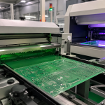
The global electronics industry is undergoing a major transformation as manufacturers face increasing pressure to improve environmental performance without sacrificing electrical performance, reliability, or production efficiency. Printed circuit boards (PCBs), which form the foundation of modern electronic products, are at the center of this transition.
From smartphones, electric vehicles, and medical equipment to industrial automation, telecommunications, artificial intelligence, and renewable-energy systems, almost every modern electronic product depends on PCBs. However, traditional PCB manufacturing involves material consumption, chemical processing, water usage, energy consumption, and manufacturing waste. As electronic products become more widespread, the need to reduce their environmental footprint has become increasingly important.
This has accelerated the development of sustainable PCB manufacturing, green PCB production, and eco-friendly PCB materials.
Rather than simply replacing one material with another, sustainable PCB production takes a broader approach that considers material selection, chemical management, energy efficiency, water consumption, waste reduction, recycling, product reliability, and end-of-life treatment.
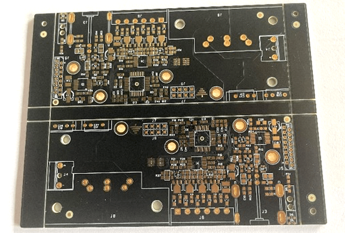
This article explores the major developments shaping the sustainable PCB industry, including environmentally preferable materials, green manufacturing processes, regulatory requirements, circular-economy strategies, and how Kingda supports customers looking for more responsible PCB and PCBA manufacturing solutions.
What Is a Sustainable PCB?
A sustainable PCB is a printed circuit board designed and manufactured with greater consideration for environmental impact throughout its lifecycle.
This can involve:
- Eco-friendly PCB materials
- Lead-free PCB assembly
- Halogen-free materials
- Reduced chemical consumption
- Water recycling and wastewater treatment
- Energy-efficient production
- Manufacturing waste reduction
- Material recovery and recycling
- Responsible supply-chain management
- Longer product operating life
Sustainability should not be treated as a single production step. Instead, it should be considered throughout the entire lifecycle:
Material Selection → PCB Design → Fabrication → PCB Assembly → Product Use → Maintenance → Recycling → End of Life
A practical sustainable PCB strategy therefore seeks to balance four major objectives:
Environmental Performance + Electrical Performance + Manufacturing Reliability + Lifecycle Cost
This balance is especially important for high-reliability products. An environmentally preferable material that cannot maintain the required thermal, mechanical, or electrical performance may not be the best overall choice for a long-life product.
Traditional PCB Materials and Their Environmental Challenges
For decades, conventional PCB manufacturing has relied heavily on fiberglass-reinforced epoxy laminates, copper, soldering materials, chemical processing solutions, and protective coatings.
Many of these materials remain highly practical and reliable, but they can create environmental challenges when production and disposal are poorly managed.
Lead and Hazardous Substances
Lead has historically been used in solder alloys because of its favorable processing characteristics. Modern electronics manufacturing, however, increasingly relies on lead-free soldering systems.
The EU’s RoHS Directive restricts certain hazardous substances in electrical and electronic equipment, while the WEEE framework promotes collection and recycling of electronic waste.
For manufacturers serving global markets, environmental compliance is therefore closely connected to material selection, supply-chain control, production documentation, and product design.
Halogenated Materials
Certain flame-retardant systems have historically relied on halogen-containing chemistry. As environmental requirements become more demanding, halogen-free PCB materials are becoming increasingly relevant in applications where customers or markets impose low-halogen requirements.
Engineers should still evaluate thermal performance, flame-retardancy requirements, dielectric properties, manufacturability, and cost before changing material systems.
Chemical Processing
PCB fabrication involves a variety of controlled chemical operations, including:
- Copper etching
- Surface preparation
- Photoresist development
- Electroless copper deposition
- Electrolytic copper plating
- Surface finishing
- Cleaning
For this reason, environmental performance depends not only on the PCB substrate but also on how the manufacturing facility handles chemicals, wastewater, emissions, and process waste.
Eco-Friendly Materials in Sustainable PCB Manufacturing
Material science is an important part of the industry’s sustainability transition.
Lead-Free Solder
Lead-free PCB assembly is now widely used for products that must satisfy applicable environmental requirements.
Common lead-free solder systems include tin-based alloys containing materials such as silver and copper.
However, lead-free soldering generally requires higher process temperatures than traditional SnPb soldering. Therefore, successful implementation requires appropriate:
- Solder-paste selection
- PCB surface finish
- Reflow-profile development
- Component temperature control
- Moisture management
- Inspection procedures
Sustainability and manufacturing quality must therefore be addressed together.
Halogen-Free PCB Materials
Halogen-free PCB materials are designed to reduce the use of certain halogen-containing flame-retardant systems.
For applications requiring low-halogen construction, manufacturers may select specialized laminate systems while maintaining appropriate:
- Tg
- CTE
- Dielectric constant
- Dissipation factor
- Thermal reliability
- Flame performance
Base-material standards such as IPC-4101 provide a framework for rigid and multilayer PCB laminate and prepreg requirements, while IPC separately identifies materials for high-speed and high-frequency applications.
Recyclable and Bio-Based PCB Materials
Researchers are also developing:
- Recyclable PCB substrates
- Bio-based PCB materials
- Cellulose-based substrates
- Bio-derived resin systems
- More easily separable multilayer constructions
These materials may be particularly attractive for low-power, disposable, temporary, or environmentally sensitive electronics.
However, many emerging technologies are still developing and may not yet provide the same combination of thermal stability, mechanical strength, moisture resistance, and high-frequency performance as established PCB materials.
For demanding applications such as automotive, aerospace, medical, RF, and high-power electronics, material qualification remains essential.
Green Manufacturing Practices for PCB Production
Sustainable PCB manufacturing is not limited to material selection. The production process itself plays a major role.
1. Chemical Management and Process Recycling
Advanced manufacturing facilities can improve environmental performance by optimizing chemical usage and increasing process recovery.
Potential approaches include:
- Automated chemical dosing
- Process monitoring
- Chemical recovery
- Closed-loop treatment systems
- Wastewater treatment
- Controlled chemical storage
- Process bath-life management
These measures help reduce unnecessary consumption while improving production consistency.
2. Water Conservation
Water is used extensively in wet PCB manufacturing processes.
A modern green PCB factory can improve water efficiency through:
- Counter-current rinsing
- Closed-loop water recycling
- Filtration systems
- Wastewater purification
- Process-flow optimization
- Automated water monitoring
Water management is particularly important because sustainability involves not only carbon emissions but also responsible resource consumption.
3. Energy Efficiency
PCB manufacturing and assembly require significant energy for:
- Lamination presses
- Plating systems
- Reflow ovens
- Compressors
- HVAC systems
- Lighting
- Drying and curing
- Cleanroom environments
Energy-efficient equipment, optimized production scheduling, preventive maintenance, and smart factory systems can reduce unnecessary energy consumption.
4. Waste Reduction
Manufacturing waste can be reduced by improving:
- Panel utilization
- PCB yield
- Process stability
- Material planning
- Production scheduling
- Scrap control
- Rework management
Better yield is both an environmental and economic advantage.
A simple relationship illustrates the point:
Higher Yield → Less Scrap → Lower Material Consumption → Lower Manufacturing Cost
5. Water-Based and Low-VOC Materials
The industry is also exploring water-based PCB inks and lower-VOC formulations for appropriate applications.
Compared with solvent-intensive alternatives, water-based systems can reduce reliance on volatile organic compounds and simplify certain cleaning processes.
However, material substitution should always be validated for:
- Adhesion
- Print quality
- Curing
- Chemical resistance
- Moisture resistance
- Thermal stability
- Long-term reliability
The Role of Process Optimization and Automation
Automation contributes to sustainability by improving consistency and reducing unnecessary material usage.
Modern PCB manufacturing systems can monitor:
- Temperature
- Pressure
- Chemical concentration
- Plating parameters
- Reflow profiles
- Production yield
- Equipment status
Real-time monitoring allows manufacturers to identify deviations early rather than producing large quantities of defective boards.
Automated inspection systems such as SPI, AOI, and X-ray inspection can further reduce rework and scrap by detecting problems earlier in the manufacturing process.
This creates a positive cycle:
Better Process Control → Fewer Defects → Less Rework → Less Waste → Higher Yield
Regulatory and Standards Landscape
Environmental regulations are becoming an increasingly important part of PCB manufacturing strategy.
RoHS
The European Union’s RoHS Directive restricts specified hazardous substances in electrical and electronic equipment. It has been a major driver for lead-free and environmentally responsible electronics manufacturing.
WEEE
The WEEE Directive focuses on the collection, recovery, and recycling of waste electrical and electronic equipment. Together with RoHS, it has influenced how electronics companies consider environmental impacts throughout the product lifecycle.
ISO 14001
ISO 14001 provides a framework for environmental management systems.
Importantly, the current edition is now ISO 14001:2026, published in April 2026. The standard provides a systematic framework for managing environmental responsibilities, compliance obligations, environmental objectives, resource use, waste, and continual improvement.
For PCB manufacturers, an environmental management system can help integrate sustainability into everyday operational decision-making rather than treating it as a standalone initiative.
IPC Standards
IPC standards continue to provide important technical frameworks for PCB materials, fabrication, design, assembly, and reliability.
For example, IPC-4101 covers base materials for rigid and multilayer printed boards, while IPC identifies IPC-4103 for high-speed/high-frequency base materials.
Environmental compliance therefore works best when integrated with established engineering and quality standards rather than treated separately.
Sustainable PCB Design: Start Sustainability Before Manufacturing
Environmental performance should begin during PCB design.
A sustainable PCB design can consider:
Material Utilization
Smaller board dimensions can reduce laminate and copper consumption, provided electrical, thermal, and mechanical requirements remain satisfied.
Panelization
Optimizing the arrangement of multiple boards on a manufacturing panel can improve material utilization and reduce production waste.
Component Lifecycle
Selecting components with stable availability can reduce redesigns caused by premature obsolescence.
Repairability
Where appropriate, designs that support repair or module replacement can extend product life and reduce electronic waste.
Thermal Management
Better thermal design can extend product lifetime, reducing replacement frequency and therefore reducing lifecycle environmental impact.
Manufacturing Yield
Designing within the manufacturer’s validated process window can reduce scrap and rework.
This is why Design for Manufacturing (DFM) and Design for Assembly (DFA) can contribute to sustainability in addition to cost and quality.
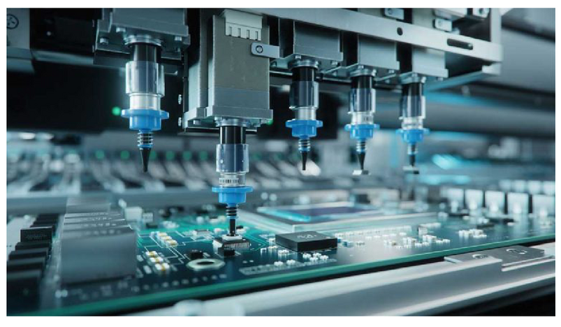
Circular Economy and the Future of PCB Manufacturing
The traditional electronics model is often described as:
Extract → Manufacture → Sell → Use → Discard
The circular-economy approach aims to move toward:
Design → Manufacture → Use → Repair → Recover → Reuse → Recycle
For PCB manufacturers, this could involve:
- Recyclable substrate systems
- Improved material separation
- Copper recovery
- Precious-metal recovery
- Component reuse
- Product refurbishment
- Longer product life
- Design for disassembly
Although completely recyclable complex PCBs remain challenging, the direction is clear: lifecycle thinking will become increasingly important in electronics manufacturing.
Challenges of Sustainable PCB Manufacturing
The move toward greener PCB production is not without difficulties.
Performance vs. Sustainability
Some emerging materials may not yet offer the same:
- Thermal resistance
- Moisture resistance
- Mechanical durability
- High-frequency performance
- Dimensional stability
as mature conventional materials.
Higher Material Costs
New environmentally preferable materials may be more expensive because production volumes remain relatively small.
Supply Availability
A sustainable material strategy is only practical if materials can be sourced consistently throughout the product lifecycle.
Qualification Requirements
Any new material must be validated through appropriate electrical, thermal, mechanical, reliability, and assembly testing.
Therefore, sustainable manufacturing should be based on engineering evidence rather than environmental claims alone.
Kingda’s Approach to Sustainable PCB Manufacturing
For OEMs and electronics companies, achieving sustainability requires a manufacturing partner capable of combining environmental management with engineering, fabrication, assembly, and quality control.
Kingda is a one-stop PCB and PCBA manufacturing provider integrating PCB manufacturing, component procurement, SMT, DIP, finished-product assembly, and testing. Its integrated manufacturing model helps reduce supplier handoffs and coordinate production through a single manufacturing workflow.
Environmental Management and Compliance
Kingda’s published information includes ISO 14001 environmental management among its manufacturing and compliance capabilities.
An environmental-management framework can support structured control of resource usage, waste, environmental objectives, and continual improvement.
The latest ISO 14001 edition, ISO 14001:2026, specifically emphasizes environmental performance, compliance obligations, resource optimization, and continuous improvement.
Advanced PCB Manufacturing Capability
Kingda supports a broad range of PCB technologies, including:
- Multilayer PCB
- HDI PCB
- High-frequency PCB
- High-speed PCB
- Controlled-impedance PCB
- High-Tg PCB
- Heavy-copper PCB
- Metal-core PCB
- Flexible PCB
- Rigid-flex PCB
- Blind and buried via PCB
Kingda’s published PCB manufacturing capability covers up to 80-layer PCB fabrication in its stated production capability, with advanced technologies including HDI, microvias, controlled impedance, and heavy copper.
These capabilities allow engineers to select materials and structures according to actual product requirements instead of using a one-size-fits-all PCB construction.
One-Stop PCB and PCBA Manufacturing
Kingda provides an integrated workflow covering:
PCB Design → PCB Fabrication → Component Procurement → SMT → THT/DIP → Testing → Finished-Product Assembly
This approach helps reduce supplier coordination, unnecessary logistics, duplicated packaging, and communication gaps.
Quality Control and Traceability
Sustainable production must also maintain strong quality control.
Kingda publishes inspection and testing capabilities including:
- SPI
- AOI
- X-ray
- FAI
- ICT
- FCT
- Electrical testing
- Functional verification
Its published PCBA information also describes manufacturing records and traceability systems supporting product lifecycle management and quality assurance.
Reducing defects, rework, and scrap is itself an important part of sustainable manufacturing.
Prototype-to-Mass-Production Support
Kingda supports a manufacturing path from rapid prototype through low-volume and larger-scale production.
This continuity can help companies maintain consistent materials, processes, inspection requirements, and engineering knowledge as production volumes increase. Kingda’s published rapid prototyping service supports no-MOQ prototype assembly, SMT and through-hole assembly, and rapid-turn production, with AOI and X-ray inspection capabilities.
Practical Strategies for Building a Sustainable PCB Program
Companies starting a sustainable PCB initiative can use the following framework:
1. Establish Environmental Objectives
Define measurable priorities such as:
- Lower chemical consumption
- Reduced water usage
- Reduced energy consumption
- Lower production waste
- Improved material recyclability
2. Evaluate PCB Materials
Select laminates, solder systems, coatings, and other materials according to both environmental and technical requirements.
3. Optimize PCB Design
Use DFM, DFA, panelization, thermal optimization, and efficient board geometry to improve yield and resource utilization.
4. Validate New Materials Through Prototypes
Before volume production, test alternative materials through controlled prototype and low-volume builds.
5. Monitor Manufacturing Data
Track:
- Yield
- Scrap
- Rework
- Energy use
- Material consumption
- Water consumption
- Process deviations
What gets measured can be improved.
6. Consider the Entire Lifecycle
Sustainability should extend beyond the factory.
Consider how the product will be:
Manufactured → Distributed → Used → Repaired → Upgraded → Recovered → Recycled
Conclusion
The transition toward sustainable PCB manufacturing is changing how the electronics industry approaches materials, production processes, environmental management, and product lifecycle planning.
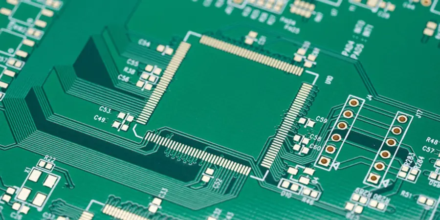
The most effective green PCB production strategy is not based on a single material or technology. Instead, it combines:
Eco-Friendly Materials + Lead-Free Assembly + Chemical Management + Water Conservation + Energy Efficiency + Waste Reduction + Recycling + Process Optimization
At the material level, halogen-free PCB materials, recyclable substrates, bio-based materials, water-based inks, and environmentally preferable coatings are creating new opportunities for greener electronics. At the factory level, automation, process monitoring, recycling, energy efficiency, and environmental management systems are helping manufacturers reduce resource consumption and waste.
At the same time, sustainability must remain compatible with reliability. A PCB must still meet its electrical, thermal, mechanical, safety, and lifecycle requirements. This makes engineering validation and manufacturing discipline essential.
With its integrated PCB fabrication, component sourcing, SMT/THT assembly, testing, traceability, and production capabilities, Kingda provides a practical platform for companies looking to combine PCB quality, manufacturing efficiency, and environmental responsibility in one supply chain.
As electronics continue to expand into AI, electric vehicles, medical technology, industrial automation, telecommunications, and smart infrastructure, sustainability will become increasingly important. Manufacturers that integrate environmental responsibility with strong engineering and manufacturing capabilities will be better positioned for the next stage of electronics innovation.