As electronics become deeply integrated into transportation, healthcare, communications, industrial automation, artificial intelligence, and consumer products, the environmental impact of electronics manufacturing is receiving greater attention.
Printed circuit boards (PCBs) are fundamental to almost every electronic system, but conventional PCB manufacturing involves materials, chemicals, water, and energy-intensive processes. As a result, manufacturers are under increasing pressure to reduce waste and emissions while maintaining electrical performance, reliability, and production efficiency.
This has accelerated the development of green PCB production and eco-friendly PCB manufacturing.
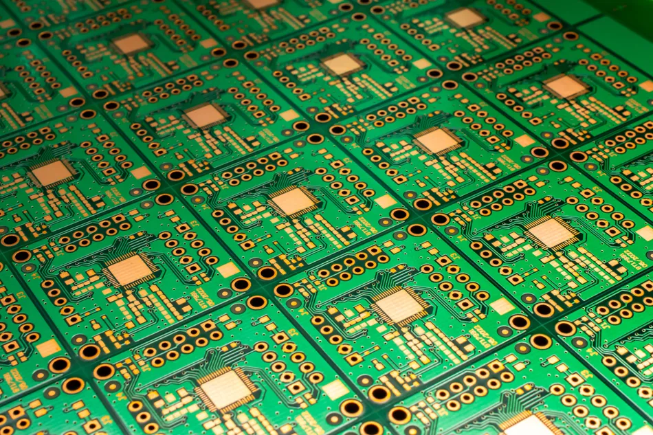
Modern sustainable manufacturing strategies focus on reducing chemical consumption, improving water efficiency, increasing material recovery, using environmentally preferable materials, reducing production waste, and improving energy efficiency. At the same time, regulations and customer requirements such as RoHS and REACH are encouraging electronics manufacturers to build stronger environmental management systems.
This guide explains the environmental impact of conventional PCB production, how green PCB manufacturing reduces pollution, the role of sustainable materials, the challenges of environmentally responsible PCB production, and how manufacturers such as Kingda can support more sustainable electronics manufacturing.
Understanding the Environmental Impact of Traditional PCB Production
Traditional PCB manufacturing involves multiple processes, including material preparation, imaging, etching, lamination, drilling, plating, surface treatment, solder-mask application, and final inspection.
Although these processes are highly controlled in professional facilities, they can consume significant amounts of resources.
The main environmental considerations include:
Chemical Consumption
PCB fabrication uses chemical processes for:
- Copper etching
- Surface preparation
- Electroless copper deposition
- Electrolytic plating
- Photoresist development
- Surface finishing
- Cleaning
If chemical management and wastewater treatment are inadequate, manufacturing waste can create environmental risks.
For this reason, modern eco-friendly PCB manufacturing places strong emphasis on chemical management, wastewater treatment, process recycling, and responsible waste disposal.
Water Consumption
Water is used in multiple PCB manufacturing operations, particularly rinsing and cleaning.
Without proper treatment and recycling, these processes can generate substantial wastewater streams. Modern manufacturers therefore increasingly use:
- Water recycling systems
- Closed-loop process systems
- Wastewater treatment
- Counter-current rinsing
- Process-water monitoring
These approaches allow factories to reduce freshwater consumption while maintaining manufacturing quality.
Energy Consumption
PCB manufacturing and assembly require electricity and thermal energy for processes such as:
- Lamination
- Reflow soldering
- Plating
- Curing
- Drying
- Air compression
- HVAC and cleanroom operation
Improving equipment efficiency and production management can therefore contribute significantly to reducing the environmental footprint of PCB manufacturing.
Manufacturing Waste
PCB production generates different types of waste, including:
- Copper scrap
- Laminate offcuts
- Drilling debris
- Photoresist waste
- Chemical residues
- Packaging materials
- Defective boards
A strong sustainable PCB manufacturing strategy aims to minimize waste at the source while improving recycling and material recovery.
What Is Green PCB Production?
Green PCB production refers to the use of environmentally responsible materials, processes, equipment, and management practices to reduce the environmental impact of printed circuit board manufacturing.
It is not simply about replacing conventional PCB materials with “green” alternatives.
A comprehensive green PCB manufacturing strategy can include:
Material Optimization → Chemical Reduction → Water Recycling → Energy Efficiency → Waste Reduction → Recycling → Environmental Compliance → Lifecycle Management
The goal is to maintain the required:
- Electrical performance
- Mechanical strength
- Thermal stability
- Manufacturing yield
- Product reliability
- Regulatory compliance
while reducing environmental impact throughout the product lifecycle.
How Eco-Conscious PCB Manufacturing Reduces Pollution
One of the biggest advantages of eco-friendly PCB manufacturing is its potential to reduce pollution at multiple stages of production.
1. Better Chemical Management
Modern PCB factories can reduce environmental risks through:
- Chemical recycling
- Automated chemical dosing
- Process monitoring
- Closed-loop systems
- Wastewater treatment
- Controlled chemical storage
Instead of treating chemicals as disposable production inputs, manufacturers can manage them as controlled process resources.
This approach can improve both environmental performance and process consistency.
2. Lead-Free PCB Assembly
Lead-free PCB assembly is an important part of environmentally responsible electronics manufacturing.
Lead-free solder systems such as SAC alloys are widely used in modern electronics to reduce dependence on lead-containing solder.
However, lead-free assembly requires appropriate thermal-process control because its soldering temperature profile differs from traditional SnPb processes.
The environmental benefit must therefore be combined with:
- Correct solder-paste selection
- Accurate stencil printing
- Controlled reflow profiles
- Proper component thermal management
- Inspection and testing
3. Waste Recovery and Recycling
Copper is one of the most valuable materials contained in a PCB.
Manufacturers can recover material from:
- Copper-clad laminate waste
- Etching processes
- Drilling operations
- PCB scrap
- Production offcuts
Recovering materials reduces the demand for virgin resources and helps move electronics manufacturing toward a more circular model.
4. Lower VOC Manufacturing
Some conventional inks and coatings rely on solvent-based chemistry.
Using water-based PCB inks, low-VOC materials, and environmentally preferable coatings can reduce solvent emissions and improve workplace conditions where technically appropriate.
Water Conservation in Green PCB Manufacturing
Water management is a critical element of sustainable PCB manufacturing.
Rather than treating wastewater as an unavoidable byproduct, environmentally responsible factories can implement systems that reduce water consumption and improve recovery.
Water Recycling
Recycling process water can reduce demand for fresh water in appropriate manufacturing applications.
Possible systems include:
- Filtration
- Chemical treatment
- Membrane purification
- Reverse osmosis
- Closed-loop rinsing
The specific approach depends on water chemistry, production processes, local environmental regulations, and required quality.
Optimized Rinsing
Rinsing is necessary for many wet PCB processes, but inefficient rinsing can consume unnecessary amounts of water.
Manufacturers can optimize:
- Spray pressure
- Flow rates
- Nozzle configuration
- Rinse sequencing
- Counter-current rinsing
This improves resource efficiency without compromising PCB cleanliness.
Wastewater Treatment
A professional PCB manufacturing facility should have controlled procedures for wastewater treatment and monitoring.
This is particularly important for processes involving metals and chemical solutions.
Effective treatment helps prevent untreated manufacturing waste from entering surrounding water systems.
Sustainable Materials for PCB Manufacturing
Material selection plays an increasingly important role in green PCB production.
Traditional FR-4 remains one of the most practical materials for many applications, but manufacturers are also exploring alternative material strategies.
Halogen-Free PCB Materials
Halogen-free PCB materials can reduce reliance on certain halogen-containing flame-retardant systems.
These materials are increasingly specified for environmentally conscious electronic products.
They can be particularly attractive when customers require:
- RoHS compliance
- Environmental product requirements
- Low-halogen specifications
- International market access
However, engineers still need to verify:
- Tg
- CTE
- Dk
- Df
- Thermal reliability
- Mechanical properties
- Assembly compatibility
Bio-Based PCB Materials
Bio-based PCB materials incorporate renewable resources into selected resin or substrate systems.
Potential benefits include:
- Reduced dependence on fossil-based raw materials
- Renewable feedstocks
- Potentially lower lifecycle impact
However, bio-based materials should be evaluated according to actual product requirements rather than material origin alone.
Recyclable PCB Materials
Research into recyclable PCB materials aims to make it easier to separate and recover materials such as:
- Copper
- Resin
- Substrate
- Electronic components
These technologies may become increasingly important as electronics manufacturers move toward circular-economy models.
Biodegradable PCB Substrates
Biodegradable PCB substrates are an emerging technology for specialized applications such as:
- Temporary sensors
- Disposable electronics
- Smart packaging
- Agricultural sensing
- Educational electronics
They are not currently a universal replacement for conventional high-performance PCB materials.
For automotive, aerospace, medical, high-frequency, and high-temperature electronics, engineers must prioritize reliable performance and validated manufacturing compatibility.
Eco-Friendly PCB Coatings
Protective coatings can help protect PCBs against:
- Moisture
- Dust
- Corrosion
- Chemicals
- Condensation
Traditional solvent-based coatings can contribute to VOC emissions.
As a result, eco-friendly PCB coatings and low-VOC coating technologies are receiving greater attention.
Potential alternatives include:
- Water-based coatings
- Low-VOC conformal coatings
- Bio-derived coatings
- Solvent-reduced protective systems
Engineers should evaluate coatings based on:
- Dielectric strength
- Adhesion
- Temperature resistance
- Chemical resistance
- Moisture protection
- UV resistance
- Rework requirements
Sustainability should never be considered separately from product reliability.
Water-Based PCB Inks
Water-based PCB inks can reduce dependence on solvent-heavy printing processes.
They may be used for applications such as:
- PCB markings
- Silkscreen printing
- Identification graphics
- Selected solder-mask systems
Potential benefits include:
- Lower VOC emissions
- Reduced solvent consumption
- Easier cleanup
- Lower hazardous waste generation
- Improved working conditions
Before switching materials, manufacturers should verify print resolution, adhesion, curing behavior, abrasion resistance, moisture resistance, and compatibility with the existing PCB production line.
Green PCB Manufacturing and Product Reliability
An important principle in sustainable electronics is that environmental performance cannot come at the expense of product reliability.
A PCB that fails prematurely may create greater environmental impact because it requires:
- Replacement products
- Additional manufacturing
- Additional transportation
- Warranty service
- Rework
- Disposal
Therefore, the right question is not:
“Which PCB material is the most environmentally friendly?”
The better question is:
“Which material and manufacturing process provides the best balance between environmental impact, reliability, manufacturability, and lifecycle performance?”
For example, a durable PCB that operates reliably for many years may have a lower overall environmental impact than a supposedly greener material that fails prematurely.
This makes lifecycle thinking essential to modern sustainable PCB manufacturing.
Benefits of Green PCB Production for Businesses
Sustainable PCB manufacturing can deliver benefits beyond environmental protection.
Reduced Operating Costs
Energy-efficient equipment, process optimization, waste reduction, and water recycling can reduce long-term manufacturing expenses.
Regulatory Compliance
Environmental management supports compliance with regulations and customer requirements such as:
- RoHS
- REACH
- Environmental material declarations
- Customer-specific substance restrictions
Improved Brand Reputation
Sustainability has become increasingly relevant for OEMs and electronics brands.
Manufacturers that can demonstrate responsible material management, waste reduction, and environmental controls can provide greater confidence to customers.
Supply Chain Resilience
Reducing dependency on specific raw materials and improving material recovery can strengthen supply chain resilience.
Higher Manufacturing Efficiency
Environmental optimization and manufacturing optimization often overlap.
For example:
Less scrap = lower material consumption + higher yield + lower cost
Lower energy use = lower environmental impact + lower operating cost
Better process control = fewer defects + less rework + less waste
Challenges of Implementing Green PCB Production
Despite its advantages, adopting green PCB production presents several challenges.
Higher Initial Investment
Environmental technologies may require investment in:
- Wastewater treatment
- Recycling systems
- Energy-efficient equipment
- Environmental monitoring
- Cleaner process technologies
The return on investment may take time.
Material Performance Limitations
Some emerging sustainable materials may not yet match advanced conventional PCB materials in:
- Thermal resistance
- Mechanical strength
- High-frequency performance
- Dimensional stability
Supply Chain Availability
Certain sustainable laminates, coatings, and inks are available from fewer suppliers than mainstream materials.
This can increase:
- Lead time
- Material cost
- Supply risk
Manufacturing Qualification
Any new material must be validated against:
- PCB fabrication process
- SMT process
- Reflow temperature
- Surface finish
- Conformal coating
- Product reliability requirements
A green material that cannot be manufactured consistently at production scale is not a practical solution.
Future Trends in Eco-Conscious PCB Manufacturing
The future of green PCB manufacturing is likely to involve several important developments.
Circular PCB Manufacturing
The electronics industry is increasingly exploring a circular approach:
Design → Manufacturing → Use → Recovery → Recycling → Reuse
This model aims to extend material value beyond the first product lifecycle.
Advanced Recycling Technologies
Future processes may improve the separation and recovery of:
- Copper
- Precious metals
- Resins
- Substrate materials
- Electronic components
Digital Manufacturing
Digital production systems can improve:
- Material tracking
- Process monitoring
- Energy management
- Predictive maintenance
- Production yield
- Waste reduction
Sustainable Materials
Bio-based, recyclable, halogen-free, and lower-impact material technologies will continue to develop as performance improves and economies of scale increase.
Sustainable PCBA
Sustainability is also moving beyond bare PCB fabrication into PCB assembly.
Future sustainable PCBA strategies may include:
- Lead-free assembly
- Low-VOC materials
- Energy-efficient reflow
- Optimized component sourcing
- Reduced packaging
- Material traceability
- Product refurbishment
- End-of-life recovery
How to Build a More Sustainable PCB Project
Engineers and procurement teams can begin with several practical steps.
Step 1: Define Environmental Objectives
Determine which factor is most important:
- Reduced hazardous substances
- Lower carbon footprint
- Water conservation
- Material recyclability
- Lower VOC emissions
- Reduced waste
Step 2: Match Materials to the Application
Evaluate:
- Temperature
- Humidity
- Electrical frequency
- Mechanical stress
- Required lifetime
- Thermal performance
- Compliance requirements
Step 3: Optimize PCB Design
A better PCB design can reduce environmental impact by improving:
- Material utilization
- Panelization
- Component density
- PCB size
- Copper usage
- Manufacturing yield
Step 4: Prototype Before Scaling
A PCB prototype allows teams to test sustainable materials and manufacturing processes before committing to volume production.
Prototype validation may include:
- Electrical testing
- Thermal cycling
- Humidity testing
- Mechanical testing
- Solderability testing
- Reliability testing
Step 5: Evaluate the Entire Lifecycle
Consider the complete product journey:
Raw Materials → PCB Manufacturing → PCBA → Product Use → Maintenance → Recycling → End of Life
This provides a more accurate assessment of environmental performance.
Kingda’s Green PCB Manufacturing and PCBA Advantages
For manufacturers and OEMs seeking a reliable partner for environmentally conscious electronics production, supplier capability is just as important as material selection.
Kingda operates as a one-stop PCB and PCBA manufacturer, integrating PCB design support, PCB fabrication, component procurement, SMT assembly, DIP/THT assembly, testing, finished-product assembly, and related manufacturing services. (Kingda)
Environmental Management and Compliance
Kingda’s published information identifies ISO 14001 environmental management, along with RoHS and REACH compliance, as part of its sustainability and manufacturing framework. (Kingda)
This provides customers with a manufacturing platform that considers both production quality and environmental requirements.
One-Stop PCB Manufacturing
Kingda combines:
PCB Fabrication → Component Procurement → SMT → DIP/THT → Inspection → Testing → Finished Product Assembly
This integrated model reduces supplier handoffs and can simplify coordination across the manufacturing lifecycle. (Kingda)
Advanced PCB Manufacturing Capability
Kingda’s published PCB capabilities include:
- Multilayer PCB
- HDI PCB
- High-speed PCB
- High-frequency PCB
- High-Tg PCB
- Heavy-copper PCB
- Flexible PCB
- Rigid-flex PCB
- Metal-core PCB
- Controlled-impedance PCB
Its published capability range extends from standard boards to advanced high-density constructions. (Kingda)
Strong PCBA and Inspection Capability
Kingda’s PCBA capabilities include full turnkey, partial turnkey, and consigned assembly, supporting SMT and through-hole technologies. Its inspection capabilities include SPI, AOI, X-ray, FAI, ICT, and FCT. (Kingda)
Full Manufacturing Traceability
Kingda reports an ERP-based manufacturing system capable of supporting product traceability throughout the production process. This can help customers connect material, manufacturing, quality, and shipment information for better process control. (Kingda)
Prototype to Mass Production
A sustainable PCB program often requires multiple development stages.
Kingda supports customers from:
PCB Prototype → Low-Volume Production → Pilot Production → Mass Production
This allows material and process decisions to be evaluated before production volumes increase. (Kingda)
Conclusion: Building a More Sustainable Electronics Industry
Green PCB production is becoming an important part of the transformation toward more sustainable electronics manufacturing.
The environmental impact of PCB production can be reduced through a combination of:
Cleaner Materials + Chemical Management + Water Recycling + Energy Efficiency + Waste Reduction + Recycling + Process Control + Environmental Compliance
Technologies such as biodegradable PCB substrates, recyclable PCB materials, halogen-free laminates, eco-friendly PCB coatings, and water-based PCB inks provide new opportunities for reducing environmental impact.
However, sustainability should never be separated from engineering fundamentals.
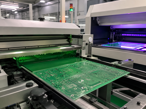
The most effective eco-friendly PCB manufacturing strategy is one that balances environmental performance with electrical reliability, thermal stability, manufacturability, regulatory compliance, and product lifetime.
For OEMs and electronics companies, this means working with manufacturing partners that can support not only green materials, but also PCB fabrication, PCBA, testing, traceability, quality control, and production scaling.
With its integrated PCB and PCBA manufacturing capabilities, environmental-management framework, engineering support, quality systems, and traceability infrastructure, Kingda provides a practical manufacturing platform for companies developing more sustainable electronic products. (Kingda)