PCB Panelization: Process Edge, Tooling Hole and Fiducial Mark Design Guidelines
When designing a PCB for automated manufacturing, panelization and positioning features must be considered before production. Properly designed PCB panelization improves board stability during manufacturing, supports accurate positioning during SMT assembly, and reduces the risk of damage during depanelization.
Among the most important design elements are the PCB process edge, tooling holes, and fiducial marks. These features provide mechanical support and positioning references for automated production equipment.
For manufacturers offering integrated PCB fabrication and assembly, these details are particularly important because PCB manufacturing and assembly processes must work together. You can learn more about professional PCB manufacturing services and available board technologies from GOPCBA.
Why Are PCB Process Edges Required?
A process edge, also called a manufacturing edge or panel edge, is an additional strip of PCB material attached to the main board during panelization.
The primary purpose of a process edge is to provide a stable area for:
- PCB handling during production
- Automated machine positioning
- SMT conveyor transportation
- Fiducial mark placement
- Tooling hole placement
- Board support during component assembly
- Automated depanelization
Although a PCB can sometimes be manufactured without a process edge, automated production lines generally require suitable mechanical support and positioning features.
For this reason, a well-designed PCB process edge is an important part of the manufacturing design rather than simply additional PCB material.
Recommended PCB Process Edge Design

A process edge is commonly designed with a width of approximately 5 mm, although the actual width should be determined according to the tooling holes, fiducial marks, PCB geometry, and assembly equipment.
The process edge must provide enough mechanical strength to prevent deformation or breakage during manufacturing.
If a large tooling hole is placed in a narrow process edge, the remaining material around the hole may become too thin. This is particularly risky when the hole is located in an unsupported or suspended area.
For example, if a process edge is approximately 4.5 mm wide while the tooling hole is approximately 4 mm in diameter, the remaining material may be insufficient to maintain adequate mechanical strength.
In such cases, increasing the process edge width is recommended.
How to Design PCB Tooling Holes
Tooling holes are mechanical reference holes used to accurately position the PCB or panel during manufacturing and assembly.
A typical tooling hole may have a diameter of approximately 2 mm, depending on the manufacturer’s production requirements.
The exact size should always be confirmed with the PCB manufacturer because tooling systems and assembly equipment can vary.
When designing tooling holes, consider the following factors:
- Hole diameter
- Distance from the PCB edge
- Process edge width
- Remaining material around the hole
- Whether the hole is mechanically supported
- Positioning requirements of the assembly equipment
Large holes should not be placed in narrow process edges without sufficient surrounding material.
If a 3 mm or 4 mm tooling hole is required, the process edge should generally be widened to provide sufficient structural strength.
Tooling Holes vs. Fiducial Marks
Tooling holes and fiducial marks serve different purposes in automated PCB manufacturing.
Tooling holes provide mechanical positioning references, while fiducial marks provide optical references for automated assembly equipment.
Fiducial marks are especially important for SMT production because vision systems use them to determine the precise position and orientation of the PCB before component placement.
GOPCBA provides comprehensive PCB assembly services covering SMT, through-hole, mixed-technology assembly, component sourcing, inspection, testing, and box build assembly.
How Many Fiducial Marks Are Needed?

For many panelized PCB designs, three or four fiducial marks can provide an effective reference system.
The marks should be positioned to give the vision system reliable information about the board’s X-axis, Y-axis, and rotational orientation.
Fiducial placement should also maintain sufficient clearance from the PCB edge.
A commonly used design reference is to maintain approximately 3.35 mm between the edge of the fiducial mark and the PCB edge, depending on the assembly manufacturer’s requirements.
The center-to-edge distance will therefore be larger than the edge-to-edge distance.
Because different SMT machines can have different positioning requirements, the manufacturer’s current design rules should always take priority.
Fiducial Mark Design Considerations
A fiducial mark normally consists of a circular copper pad surrounded by a clear area free from other copper features, solder mask, or silkscreen interference.
The purpose is to provide a clean optical contrast for the SMT machine’s vision system.
When designing fiducials:
- Keep the mark away from the PCB edge.
- Maintain sufficient clearance around the mark.
- Avoid placing silkscreen over or too close to the mark.
- Avoid nearby copper patterns that could confuse the vision system.
- Keep fiducial locations consistent across the panel.
- Follow the assembly manufacturer’s recommended dimensions.
For complex or high-density boards, reviewing the panel design before fabrication can prevent positioning and assembly problems.
PCB Panelization and SMT Assembly
Good PCB panelization should be designed around the complete manufacturing process rather than only the PCB fabrication stage.
A panel normally combines multiple individual boards with a supporting process edge. Depending on the board geometry, different separation methods may be used, including V-grooving, routing, or other depanelization techniques.
The panel design must provide sufficient rigidity while allowing the individual PCBs to be separated after assembly.
Poor panelization can result in:
- Process edge breakage
- PCB deformation
- Positioning errors
- SMT placement problems
- Difficult depanelization
- Mechanical damage to components
- Reduced manufacturing efficiency
For projects requiring rapid prototyping or production quantities, GOPCBA also provides Prototype PCB Assembly to support early-stage product validation and small-batch manufacturing.
Common PCB Panelization Design Problems
Oversized Tooling Holes in Narrow Process Edges
One common problem is using a large hole in a narrow process edge.
If the hole diameter approaches the width of the process edge, very little material remains around the hole. This can significantly weaken the edge.
The solution is to increase the process edge width or reduce the hole diameter where possible.
Tooling Holes in Unsupported Areas
A tooling hole located in a suspended section of the process edge can create a weak point.
During transportation or assembly, mechanical forces may cause the process edge to crack around the hole.
Tooling holes should therefore be placed in mechanically supported areas whenever possible.
Insufficient Fiducial Clearance
Fiducial marks placed too close to the board edge or surrounded by interfering copper and silkscreen may reduce the reliability of optical recognition.
Maintaining adequate clearance helps the SMT vision system identify the reference mark accurately.
Adding Positioning Features Without Considering Assembly
PCB designers sometimes add positioning features based only on PCB fabrication requirements without considering SMT assembly.
However, tooling holes and fiducial marks should be evaluated together with the panel structure, conveyor requirements, component placement, and depanelization process.
PCB Panelization for Different Production Volumes
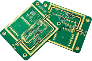
The required panel structure can vary according to production volume and manufacturing method.
For prototypes, the panel may be relatively simple and primarily intended to improve handling and assembly efficiency.
For larger production runs, the panel design should be optimized for automated SMT equipment, stable transportation, repeatable positioning, and efficient depanelization.
GOPCBA supports projects ranging from prototypes and low-volume production to large-scale manufacturing. Its PCB assembly capabilities include turnkey, partial turnkey, and consigned assembly, supporting different customer supply-chain models.
How to Improve PCB Manufacturing Reliability
Before releasing a PCB design for production, engineers should verify the following:
- Confirm the process edge width.
- Check tooling hole diameter and location.
- Make sure sufficient material remains around each hole.
- Verify fiducial mark quantity and placement.
- Check fiducial clearance from the PCB edge.
- Confirm that silkscreen and copper do not interfere with fiducial recognition.
- Review the panel separation method.
- Confirm the panel dimensions are compatible with SMT equipment.
- Review the design with the PCB manufacturer before mass production.
For projects involving complex boards, DFM review can identify manufacturing risks before fabrication. GOPCBA provides DFM and DFA services to help optimize PCB designs for manufacturing and assembly.
PCB Process Edge and Fiducial Mark Design Checklist
Before submitting your PCB files, confirm:
- The process edge is wide enough to maintain mechanical strength.
- Tooling holes do not excessively weaken the process edge.
- Large holes have sufficient surrounding material.
- Tooling holes are located in mechanically supported areas.
- Fiducial marks have sufficient clearance.
- Fiducial marks are not obstructed by silkscreen or nearby copper.
- The panel can be transported reliably through the SMT line.
- The selected depanelization method is compatible with the PCB design.
- The panel dimensions meet the assembly manufacturer’s requirements.
Final Considerations
A reliable PCB manufacturing design must consider fabrication, panelization, SMT assembly, inspection, and depanelization as one integrated process.
Proper PCB process edge design provides mechanical support, while tooling holes provide accurate mechanical positioning and fiducial marks enable reliable optical positioning during automated assembly.
By addressing these features during the PCB design stage, engineers can reduce manufacturing risks, improve SMT placement accuracy, and achieve more consistent production results.
For projects requiring complete manufacturing support, GOPCBA provides integrated PCB fabrication, component sourcing, assembly, inspection, testing, and system integration. You can contact GOPCBA to discuss your PCB manufacturing and assembly requirements.