PCB Back Drilling: How It Improves High-Speed Signal Integrity
As digital systems continue to operate at higher data rates and frequencies, maintaining signal integrity has become a critical requirement in modern PCB design. Conventional through-hole vias can introduce unwanted electrical structures that negatively affect high-speed signal transmission.
One effective solution is PCB Back Drilling, a controlled secondary drilling process that removes the unused portion of a plated through-hole via. By eliminating the unnecessary Via Stub, back drilling can reduce signal reflections, resonance, and other discontinuities that become increasingly significant in high-speed circuits.
For complex multilayer and high-speed designs, back drilling should be considered together with the PCB stack-up, via structure, impedance requirements, and overall signal-integrity strategy.
For additional manufacturing support, see our PCB Manufacturing Services.
What Is PCB Back Drilling?
A conventional plated through-hole extends through the entire PCB, even when the electrical connection only needs to reach certain layers.
For example, consider a six-layer PCB where a signal only needs to connect from Layer 1 to Layer 2. A conventional through-hole via may still extend physically from Layer 1 all the way to Layer 6. The unused portion below the signal termination point becomes a via stub.
At low frequencies, this unused structure may have limited impact. However, as signal frequency and edge rate increase, the stub can behave as an unwanted transmission-line section and contribute to:
- Signal reflection
- Impedance discontinuities
- Resonance
- Signal attenuation
- Crosstalk and electromagnetic interference
- Reduced overall signal integrity
Backdrill PCB technology addresses this problem by mechanically removing the unused section of plated copper from the via.
The process does not replace the original through-hole structure. Instead, the PCB is initially manufactured with a conventional plated through-hole, followed by a precisely controlled secondary drilling operation.
Why Is Back Drilling Important for High-Speed PCB Design?
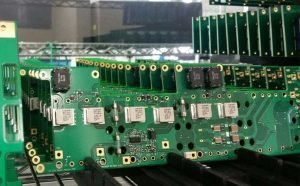
Modern interfaces such as high-speed digital links, networking systems, telecommunications equipment, servers, and high-performance computing platforms can be highly sensitive to discontinuities in the transmission path.
A via stub adds additional electrical length to the signal path. When the signal’s frequency content becomes sufficiently high, this additional structure can produce reflections and resonance.
Therefore, reducing unnecessary via length can improve the electrical characteristics of the interconnect.
Our High-Speed PCB Manufacturing capabilities and engineering approach consider stack-up, impedance, via structures, and signal-integrity requirements together rather than treating back drilling as an isolated process.
Key Benefits of PCB Back Drilling
1. Reduced Signal Noise and Interference
Removing unnecessary via stubs reduces unwanted electromagnetic effects associated with unused plated-through-hole sections.
This can help minimize signal distortion and interference in high-speed circuits.
2. Improved Signal Integrity
Back drilling creates a shorter and more electrically optimized via structure. This can reduce impedance discontinuities and reflections, helping high-speed signals travel more reliably through the PCB.
3. Better High-Frequency Performance
As operating frequencies and data rates increase, the influence of via geometry becomes more significant.
Back drilling is therefore commonly considered for high-speed and high-frequency PCB applications where conventional through-hole structures may introduce unacceptable electrical discontinuities.
4. Reduced Dependence on Blind and Buried Vias
In some designs, designers may use blind or buried vias to avoid long via stubs. Back drilling provides another option that can achieve the required electrical performance while retaining a through-hole-based structure.
This can simplify certain PCB architectures and potentially reduce manufacturing complexity compared with more advanced via structures.
Our HDI PCB Design guide provides additional information about blind vias, buried vias, microvias, and their influence on signal integrity.
How Does PCB Back Drilling Work?
Back drilling is essentially a controlled secondary drilling operation.
The typical process can be summarized as follows:
Step 1: Manufacture the Through-Hole Via
The PCB is first drilled using the required through-hole diameter. The hole is then plated so that the inner wall becomes electrically conductive.
At this stage, the via normally extends through the complete PCB thickness.
Step 2: Identify the Unused Via Section
The electrical connection is analyzed to determine which portion of the plated through-hole is unnecessary.
For example, if a signal travels from Layer 1 to Layer 3 on a six-layer board, the via section extending from Layer 3 toward Layer 6 may become the unwanted stub.
Step 3: Perform Secondary Drilling
A larger drill is used from the appropriate side of the PCB to remove the unwanted plated section.
The drilling depth must be precisely controlled so that the useful portion of the via remains intact.
Step 4: Fill the Back-Drilled Area
After back drilling, the removed section may be filled with resin according to the manufacturing process and board requirements.
Depending on the design and surface construction, additional processing such as copper capping may also be required.
Step 5: Inspect the Finished Structure
The manufacturer verifies the back-drill depth, remaining stub length, hole structure, and relevant dimensional requirements to ensure the finished PCB meets the design specifications.
PCB Back Drilling Design Guidelines
Back drilling should be incorporated into the PCB design process rather than added after the layout is completed.
Design the Via as a Through Hole
For many manufacturing workflows, the via should initially be designed as a conventional through-hole.
The manufacturer can then use additional drilling data or defined hole-size information to identify which vias require back drilling.
This approach differs from simply designing the connection as a blind via.
Clearly Identify Back-Drilled Vias
There are several ways to distinguish back-drilled holes in manufacturing data.
One common method is to create a separate drill file for the back-drilled vias.
For example:
Backdrill_L1-L2.drlBackdrill_L1-L3.drl
The naming convention should clearly identify the starting and ending layers of the back-drilling operation.
Another method is to use slightly different finished hole diameters to distinguish between standard through holes and different back-drill structures.
However, the exact method should always be confirmed with the PCB manufacturer before production.
Define the Back-Drill Depth Carefully
Back drilling requires a controlled depth because the drill must remove the unwanted copper without damaging the useful via connection.
The remaining distance between the bottom of the back-drilled hole and the adjacent PCB layer is particularly important.
For the manufacturing process described in the source specifications, a minimum dielectric distance of approximately 0.15 mm should be maintained between the back-drill bottom and the adjacent layer.
Because actual manufacturing tolerances depend on the PCB construction and process capability, designers should confirm this value with the manufacturer before finalizing the stack-up.
Back Drilling vs. Blind and Buried Vias
Back drilling, blind vias, and buried vias can all be used to reduce unnecessary via structures, but they work differently.
Back Drilling
Back drilling starts with a plated through-hole and removes the unused portion after plating.
Advantages:
- Reduces via stub length
- Supports high-speed signal transmission
- Can retain a through-hole architecture
- May reduce the need for some blind or buried vias
Blind Via
A blind via connects an outer layer to one or more internal layers without extending through the entire PCB.
Blind vias are particularly useful for high-density routing and fine-pitch BGA escape.
Buried Via
A buried via connects internal layers without reaching either external surface.
It provides additional routing flexibility but generally requires more complex PCB fabrication processes.
For high-density designs, the appropriate via technology should be selected based on electrical performance, routing density, stack-up, manufacturing capability, and cost.
How to Specify Back Drilling in PCB Manufacturing Data
Clear manufacturing documentation is essential.
A typical back-drilling specification should identify:
- Which vias require back drilling
- The drilling side
- Starting layer
- Ending layer
- Drill diameter
- Finished hole diameter
- Back-drill depth
- Required remaining stub
- Stack-up and dielectric thickness
- Resin filling requirements
- Copper capping requirements, if applicable
For complex projects, it is strongly recommended to confirm these details with the manufacturer’s engineering team before fabrication.
Our PCB Design & Layout Services can help evaluate stack-up, impedance, via structures, and manufacturing feasibility before production.
Important Considerations Before Using Back Drilling
1. Confirm the PCB Stack-Up
The layer structure determines how deep the back drill needs to go. The stack-up should therefore be finalized before the back-drill structure is defined.
2. Consider Drill Depth Tolerance
Back drilling is a depth-controlled machining process. The actual drill depth has a manufacturing tolerance, so sufficient dielectric clearance must be provided.
3. Minimize the Remaining Stub
The goal is not simply to perform a back drill but to reduce the remaining via stub to an electrically acceptable length.
The required stub length depends on the signal’s frequency content, rise time, via geometry, dielectric properties, and system-level signal-integrity requirements.
4. Coordinate With the PCB Manufacturer
Different PCB manufacturers may use different CAM processes, drill-depth controls, minimum clearances, and documentation requirements.
Engineering review before production can prevent incorrect interpretation of back-drill files.
5. Evaluate the Cost
Back drilling requires an additional drilling operation and therefore normally adds manufacturing cost.
For this reason, it should be applied selectively to vias where the electrical benefits justify the additional process.
Back Drilling for High-Speed PCB Applications
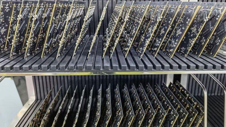
Back drilling is particularly useful for PCB designs where high-speed signals pass through multilayer structures and conventional through-hole vias create excessive stubs.
Typical applications include:
- High-speed networking equipment
- Servers and data centers
- Telecommunications equipment
- High-performance computing systems
- Industrial communication equipment
- Advanced automotive electronics
- High-speed digital interfaces
- RF and mixed-signal systems
However, back drilling is not automatically required for every high-speed PCB.
The correct solution depends on the complete interconnect structure, including trace geometry, dielectric thickness, via dimensions, signal rise time, operating frequency, reference planes, and target impedance.
Our Controlled Impedance PCB manufacturing approach can be combined with back drilling when the application requires tighter control of high-speed transmission paths.
PCB Back Drilling and Signal Integrity
The primary purpose of back drilling is to reduce the electrical impact of unnecessary via stubs.
A high-speed signal does not respond only to the schematic connection. It responds to the physical transmission path.
Therefore, PCB designers need to consider:
- Trace width
- Trace thickness
- Dielectric thickness
- Dielectric constant
- Via diameter
- Via pad size
- Anti-pad geometry
- Reference-plane configuration
- Via stub length
- Impedance requirements
Back drilling is one part of a broader signal-integrity strategy.
It should work together with proper stack-up design, controlled impedance, appropriate routing, optimized via geometry, and manufacturing process control.
Manufacturing Quality and Inspection
Because back drilling involves a controlled secondary machining process, manufacturing quality control is important.
A professional PCB manufacturer should be able to review:
- Drill depth
- Remaining stub length
- Hole diameter
- Layer registration
- Plated-hole integrity
- Resin filling
- Copper capping
- Overall board thickness
- Electrical performance
Our PCB Quality Management process includes engineering review, PCB fabrication controls, electrical testing, and quality inspection to maintain manufacturing consistency.
For complex high-speed designs, additional verification such as impedance testing, cross-section analysis, and other engineering evaluations may also be appropriate.
PCB Back Drilling vs. Standard Through-Hole Vias
The key difference is the presence of an unnecessary plated section.
A standard through-hole via remains plated through the complete PCB thickness.
A back-drilled via starts as a through-hole but has the unused portion mechanically removed after plating.
This creates a shorter effective via structure and can significantly reduce the electrical influence of the via stub.
The approach is especially valuable when the PCB must maintain a through-hole architecture while meeting high-speed signal-integrity requirements.
Conclusion
PCB Back Drilling is an effective manufacturing technique for reducing unwanted Via Stub structures in multilayer PCBs. By removing the unused portion of a plated through-hole, back drilling can reduce reflections, impedance discontinuities, resonance, and signal distortion in demanding high-speed applications.
The most important point is that back drilling should not be treated as an isolated manufacturing option. The back-drill depth, PCB stack-up, via geometry, dielectric clearance, remaining stub, impedance requirements, and manufacturing tolerances all need to be considered together.
For high-speed and high-frequency PCB projects, early collaboration between the PCB designer and manufacturer can help determine whether back drilling, blind vias, buried vias, microvias, or another interconnect structure provides the best combination of electrical performance, manufacturability, and cost.
To discuss a complex PCB project, you can contact our engineering team through PCB Manufacturing & Assembly Services or visit our Contact Us page for project support.