Single-Sided PCB Design: Simple Structure, Important Design Details
A Single-Sided PCB is one of the simplest printed circuit board structures, but its straightforward construction does not mean that design considerations can be overlooked. Single-sided boards remain widely used in applications such as radios, washing machines, remote controls, industrial equipment, and other cost-sensitive electronic products.
Unlike multilayer boards, a single-sided PCB generally has conductive copper circuitry on only one side of the substrate. This simplified structure can reduce manufacturing complexity and cost, making it suitable for electronic products with relatively uncomplicated circuit requirements.
For projects that require rapid validation or small-batch production, understanding the relationship between PCB design, fabrication, and assembly is especially important. A professional PCB Prototype manufacturer can help identify potential design and manufacturing issues before production begins.
1. Single-Sided PCB Structure
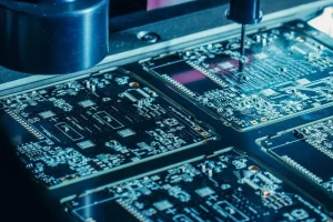
A conventional FR-4 single-sided PCB normally contains copper circuitry on one side, with solder mask and silkscreen applied according to the product’s design requirements.
Because conventional single-sided PCB manufacturing does not use the same through-hole copper-plating process as double-sided and multilayer boards, the walls of the drilled holes are generally not copper-plated.
However, actual manufacturing specifications depend on the selected board material and production process. For specific material thicknesses or special production requirements, the final structure should always be confirmed with the manufacturer before ordering.
The basic structure can therefore be understood as:
- One conductive copper layer
- One insulating substrate
- Solder mask on the circuit side
- Silkscreen where required
- Non-plated component holes for conventional through-hole components
This simple construction makes single-sided boards particularly suitable for applications where circuit density and routing complexity are relatively low.
For projects requiring more complex circuitry, customers can consider professional PCB Manufacturing solutions covering rigid, flexible, multilayer, and other specialized PCB technologies.
2. How Are Components Soldered on a Single-Sided PCB?
Because a single-sided PCB contains circuitry on only one side, component soldering must be performed on the side where the exposed copper pads are located.
The component structure determines the appropriate soldering method.
Through-Hole Component Soldering
For through-hole components, component leads pass through the PCB holes and are soldered to the copper pads on the circuit side.
This method is commonly used for components that require stronger mechanical support, larger leads, or relatively simple circuit layouts.
Component Placement and Soldering Orientation
When designing a single-sided PCB, the designer must carefully consider:
- Which side contains the copper circuitry
- Which side components are mounted from
- Where solder joints will be formed
- Whether component leads can pass through the required holes
- Whether the physical assembly orientation matches the PCB design
Incorrect layer orientation can result in a board that is electrically or mechanically different from the intended design.
For assemblies involving both surface-mount and through-hole components, a professional PCB Soldering and assembly process can provide additional engineering support and inspection.
3. Designing the PCB Manufacturing Files
A complete PCB design is normally created using multiple layers in the PCB design software. Each layer has a specific manufacturing or documentation purpose.
For a double-sided PCB, for example, the top layer is normally viewed directly from the component side. Text placed on the top layer is therefore displayed in its normal orientation.
The bottom layer, however, is viewed through the board in the design environment. If text is placed normally on the bottom layer, the corresponding text on the manufactured board will appear reversed when viewed from the opposite side.
The same principle applies to copper traces.
Bottom-Layer Routing Requires Special Attention
If a single-sided PCB uses the bottom layer for routing, designers must understand how the PCB design software represents the layer and how the finished board will be physically viewed.
This is particularly important when:
- Routing is placed on the bottom copper layer
- Component locations are defined from a specific viewing direction
- Silkscreen text is added
- Mechanical drawings are created
- Assembly instructions are prepared
Before submitting files for manufacturing, always verify the layer stack, board orientation, component placement, and manufacturing output.
For more demanding projects, PCB Prototype production provides an opportunity to verify the actual board before committing to larger quantities.
4. Manufacturing Considerations for Single-Sided PCBs
During PCB production, manufacturers may adjust the manufacturing orientation of the board to improve drilling quality and reduce burrs or other mechanical defects.
For example, when drilling holes, the relationship between the copper surface, substrate, and supporting material can influence drilling results.
Manufacturers may therefore use an appropriate production orientation or mirror the manufacturing data when necessary. Such manufacturing adjustments do not necessarily change the customer’s intended electrical design.
The purpose is to optimize the manufacturing process and achieve cleaner holes and more consistent production quality.
Why Drilling Direction Matters
During mechanical drilling, the drill bit interacts with the copper layer, substrate, and backing material. If the board is positioned incorrectly for a particular process, drilling can produce undesirable burrs or protrusions.
For this reason, professional PCB manufacturers carefully manage:
- Drill direction
- Tool selection
- Board support
- Hole diameter
- Material thickness
- Manufacturing orientation
- Deburring requirements
These considerations become even more important when very small holes or tight mechanical tolerances are involved.
5. Key Single-Sided PCB Design Tips
Although single-sided PCBs have a relatively simple structure, designers should pay close attention to several important details.
Confirm the Circuit Layer
Always confirm which physical side of the PCB contains the copper circuitry. A layer-orientation mistake can cause the final board to be effectively mirrored relative to the intended design.
Verify Component Orientation
Component placement should be checked from the actual assembly perspective. Pay particular attention to polarized components, connectors, switches, LEDs, diodes, and other components with defined orientations.
Check Drill Sizes
Component holes should be matched to the actual lead diameter and manufacturing capability. Very small holes may require additional manufacturing considerations.
Review Silkscreen Orientation
Text, logos, reference designators, and symbols should be checked carefully before production. Bottom-side information may require mirroring to appear correctly on the finished board.
Confirm the Manufacturing Data
Before submitting files, verify the Gerber files, drill files, board outline, layer definitions, and component information.
A complete engineering review can help identify potential manufacturing problems before they become expensive production issues.
6. When Should You Use a Single-Sided PCB?
A single-sided PCB is a good option when the circuit does not require high routing density or electrical interconnection between multiple copper layers.
Typical applications include:
- Simple consumer electronics
- Remote controls
- Basic industrial controllers
- Low-complexity power circuits
- Simple instrumentation
- Cost-sensitive electronic products
- Educational and hobby electronics
The main advantages include simple construction, relatively low manufacturing cost, and straightforward production.
However, when a design requires dense routing, controlled impedance, high-speed signals, numerous interconnections, or compact packaging, a double-sided or multilayer PCB may be more appropriate.
7. From PCB Prototype to Production
A single-sided PCB can be an effective solution for simple electronic designs, but successful production depends on more than simply drawing the circuit.
Designers need to consider the complete manufacturing chain, including PCB layout, material selection, drilling, soldering, component placement, inspection, and final assembly.
For development projects, a PCB Prototype can be used to verify electrical functionality and mechanical fit before production quantities are increased.
For integrated manufacturing requirements, PCB Manufacturing and assembly can be combined with component sourcing, SMT/THT assembly, inspection, testing, and other downstream processes.
Conclusion
Single-sided PCBs are simple, economical, and highly practical for many electronic applications. However, their simple construction does not eliminate the need for careful engineering.
The most important considerations are circuit-layer orientation, component placement, soldering direction, drill design, manufacturing files, and production orientation.
The key principle is simple: always design the PCB from the perspective of the finished physical product, not only from the software view.
By verifying layer orientation and manufacturing data before production, designers can avoid common mistakes such as reversed circuits, incorrect component orientation, unsuitable drill sizes, and improperly positioned silkscreen information.
For projects that require professional fabrication and assembly, working with an experienced PCB Manufacturing and assembly partner can help ensure that the design moves smoothly from prototype validation to reliable production.