HDI PCB: Structure, Types, Design, Manufacturing Process, Applications, and Benefits
High-Density Interconnect (HDI) PCB technology has become an essential solution for modern electronic products that require smaller form factors, higher component density, faster signal transmission, and improved electrical performance.
As electronic devices continue to become smaller and more powerful, conventional PCB structures can struggle to provide sufficient routing space. HDI PCB technology addresses this challenge by using advanced interconnection techniques such as laser-drilled microvias, blind vias, buried vias, sequential lamination, fine-line routing, and fine-pitch component placement.
These technologies allow designers to integrate more circuits and components into a smaller PCB footprint while maintaining electrical, mechanical, and thermal reliability.
Unlike conventional through-hole PCB structures, HDI PCBs use microvias and sequential build-up structures to establish interconnections between selected PCB layers. This provides greater routing flexibility and significantly improves space utilization.
Today, HDI PCB manufacturing is particularly important when PCB size, component density, signal integrity, electrical performance, and miniaturization are critical design requirements.
What Is an HDI PCB?
A High-Density Interconnect (HDI) PCB is a printed circuit board manufactured with a significantly higher wiring density than conventional PCB technology.
According to commonly used HDI design practices, an HDI PCB may incorporate:
- Laser-drilled microvias
- Blind vias
- Buried vias
- Sequential lamination
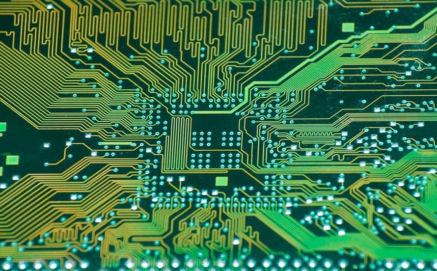
- Fine-line and fine-space traces
- Fine-pitch component pads
- High-density multilayer structures
- Via-in-pad technology
- Microvia stacking or staggering
The main purpose of these technologies is to create more electrical connections within a smaller physical area.
For example, instead of relying exclusively on large mechanically drilled through-holes, HDI PCB designs can use small laser-drilled microvias to connect adjacent or selected layers. This frees up routing space and allows components to be placed closer together.
As a result, HDI PCB design is widely used in smartphones, wearable devices, medical electronics, automotive electronics, telecommunications equipment, aerospace systems, and other compact electronic products.
Key Features of HDI PCB
HDI PCBs combine advanced interconnection structures with high-density circuit layouts to support increasingly complex electronic systems.
Microvias are significantly smaller than conventional mechanically drilled vias and can be used to establish electrical connections between adjacent or selected layers.
Depending on the design, an HDI PCB may incorporate:
- Microvias
- Stacked microvias
- Staggered microvias
- Blind vias
- Buried vias
- Through vias
These structures provide greater routing flexibility while reducing the amount of PCB real estate required for interconnections.
Fine-Line and Fine-Space Routing
Modern electronic components continue to become smaller, particularly in smartphones, wearable devices, AI hardware, and advanced semiconductor packages.
Fine-line PCB technology enables designers to route more connections within a limited area. This makes it possible to support high-density component packages without dramatically increasing PCB dimensions.
Advanced HDI manufacturers can produce extremely fine circuit geometries, although the achievable line width and spacing depend on materials, copper thickness, fabrication processes, board stack-up, and manufacturing capability.
Sequential Lamination
Sequential lamination is another important HDI manufacturing technology.
Instead of producing the entire multilayer structure in a single conventional lamination process, manufacturers can build additional dielectric and copper layers sequentially.
This approach allows more sophisticated interconnection structures and supports:
- High layer counts
- Microvia structures
- High-density routing
- Compact component placement
- Advanced semiconductor packaging
Precise registration control during sequential lamination is essential because even small alignment errors can affect via reliability and electrical performance.
Shorter Signal Paths
HDI PCB designs can reduce the physical distance between components and interconnections.
Shorter signal paths can help reduce parasitic effects, signal loss, electromagnetic coupling, and propagation delays. When combined with appropriate stack-up design and impedance control, HDI technology can support high-speed applications such as 5G communication equipment, automotive radar, AI computing hardware, and high-speed networking systems.
Improved Thermal Management
Although thermal performance depends strongly on PCB materials, copper distribution, component placement, thermal vias, and system-level cooling, HDI technology can provide designers with greater freedom to optimize thermal paths.
Thermal vias and strategically designed copper structures can help transfer heat away from high-power components and improve system stability.
Applications of HDI PCBs
HDI technology has become an important part of modern electronics across multiple industries.
Consumer Electronics
Smartphones, tablets, laptops, smartwatches, wireless devices, cameras, and other compact consumer products frequently use HDI PCB technology.
The combination of high component density and limited internal space makes HDI particularly suitable for these products.
Automotive Electronics
Automotive electronics increasingly depend on high-density and high-reliability circuit boards.
HDI PCBs can be used in:
- Advanced Driver Assistance Systems (ADAS)
- Automotive radar
- Infotainment systems
- Electric vehicle control units
- Battery management systems
- Vehicle networking
- Instrument clusters
- Advanced body electronics
Automotive HDI applications require strong process control and appropriate quality systems because circuit boards may operate under vibration, temperature cycling, humidity, and other demanding conditions.
Medical Electronics
Medical imaging systems, portable monitoring devices, diagnostic equipment, surgical electronics, and wearable medical devices can benefit from HDI technology.
The ability to reduce PCB size while maintaining complex electrical functionality is particularly valuable for portable and handheld medical equipment.
Aerospace and Defense
Aerospace and defense systems often require compact, lightweight, and highly reliable electronic assemblies.
HDI PCBs can be used in:
- Navigation systems
- Radar equipment
- Avionics
- Communication systems
- Satellite electronics
- Military electronics
- Aerospace control systems
These applications may require specialized materials, stringent inspection procedures, traceability, and industry-specific certifications.
Telecommunications and 5G
High-speed telecommunications equipment requires efficient signal routing and controlled impedance.
HDI PCB technology can support:
- 5G infrastructure
- Network switches
- Routers
- Optical communication equipment
- RF systems
- High-speed networking hardware
Industrial Automation and IoT
Robotics, sensors, industrial controllers, smart gateways, and IoT devices increasingly require compact electronics with sophisticated functionality.
HDI PCBs provide designers with greater routing density while helping reduce the size of the final electronic assembly.
Why Are HDI PCBs Important for Modern Electronics?
The electronics industry is moving toward smaller dimensions, higher processing speeds, greater functionality, and lower power consumption.
Traditional PCB structures can become increasingly difficult to route as component density rises. HDI PCB technology addresses these challenges by allowing more interconnections to be placed within a smaller area.
1. Supports Product Miniaturization
Consumers expect thinner smartphones, lighter laptops, smaller wearable devices, and increasingly compact electronic products.
HDI technology allows manufacturers to integrate more circuitry without proportionally increasing PCB size.
2. Enables Higher Circuit Density
Microvias and fine-line structures create additional routing opportunities between PCB layers.
This allows engineers to accommodate advanced components and complex circuits within limited board dimensions.
3. Supports High-Speed Signal Performance
HDI designs can reduce interconnection distances and provide greater control over routing structures.
With proper stack-up planning, impedance control, grounding, and material selection, HDI PCBs can support demanding high-speed applications.
4. Improves Design Flexibility
HDI structures give PCB designers more options for routing complex circuits.
This is particularly valuable when working with:
- Fine-pitch BGAs
- CSP packages
- Advanced processors
- High-speed memory
- RF components
- High-density connectors
5. Can Improve System Reliability
Microvias are smaller than conventional drilled vias and can provide reliable interlayer connections when properly designed and manufactured.
However, reliability depends on factors such as aspect ratio, copper plating quality, via geometry, materials, thermal cycling, and manufacturing process control.
6. Supports Efficient Thermal Design
HDI designs can incorporate thermal vias and optimized copper structures to help manage heat around high-power components.
Thermal design should nevertheless be evaluated at the system level rather than assuming that HDI construction alone automatically improves thermal performance.
Top 15 HDI PCB Manufacturers in the World in 2026
The global HDI PCB market includes manufacturers from North America, Europe, Japan, South Korea, Taiwan, China, and other major electronics manufacturing regions.
The following list is an editorial selection based on factors such as HDI technology capabilities, manufacturing scale, engineering expertise, quality systems, industry coverage, advanced packaging capabilities, and global supply-chain presence. The ranking should not be interpreted as an official industry-wide ranking.
1. TTM Technologies
TTM Technologies is one of the world’s major PCB manufacturers and has extensive capabilities in advanced interconnect technologies.
The company serves demanding markets including aerospace and defense, data networking, telecommunications, automotive, and other high-reliability applications.
Its technology portfolio extends beyond HDI PCB manufacturing to include RF and microwave PCBs, high-layer-count boards, advanced packaging, and other specialized circuit-board technologies.
Key Strengths
- Advanced multilayer HDI capabilities
- Strong aerospace and defense experience
- High-reliability manufacturing
- Advanced signal-integrity engineering
- Large-scale global manufacturing infrastructure
TTM Technologies is particularly well suited to complex and high-reliability applications where engineering capability and manufacturing consistency are critical.
2. Unimicron Technology
Unimicron Technology is a major Taiwanese PCB manufacturer with extensive experience in HDI PCBs, IC substrates, and semiconductor-related technologies.
The company supports major electronics and semiconductor supply chains and has strong capabilities in high-density multilayer circuit structures and advanced packaging.
Key Strengths
- Advanced HDI manufacturing
- High-density multilayer PCBs
- IC substrate technology
- Semiconductor packaging support
- Large-scale production capabilities
Unimicron remains an important supplier within the global electronics manufacturing ecosystem.
3. Compeq Manufacturing
Compeq Manufacturing is a major Taiwan-based PCB manufacturer serving consumer electronics, automotive electronics, networking equipment, and other markets.
Its capabilities include HDI PCBs, multilayer boards, fine-line processing, high-speed circuit technology, and impedance-controlled PCB manufacturing.
Key Strengths
- Strong smartphone PCB experience
- Advanced HDI manufacturing
- High-speed signal design
- Automotive electronics capabilities
- High-volume manufacturing
Compeq is particularly relevant to customers requiring scalable production for sophisticated electronic devices.
4. AT&S
AT&S is an Austria-based manufacturer specializing in advanced PCBs, HDI technology, IC substrates, and semiconductor packaging.
The company serves automotive, medical, industrial, aerospace, high-performance computing, and other demanding markets.
Key Strengths
- Advanced HDI and substrate technology
- Semiconductor packaging integration
- Automotive manufacturing expertise
- High-precision engineering
- European engineering and manufacturing capabilities
AT&S is particularly competitive in applications where miniaturization, electrical performance, and manufacturing precision are essential.
5. Ibiden
Ibiden is a major Japanese manufacturer known for advanced PCB and semiconductor packaging technologies.
Its capabilities include high-density interconnection, fine-line circuit manufacturing, multilayer PCB structures, and advanced thermal-management technologies.
Key Strengths
- Advanced semiconductor-related technologies
- Fine-line PCB manufacturing
- Strong R&D capabilities
- High manufacturing standards
- High-reliability applications
Ibiden has a strong position within advanced semiconductor and electronics supply chains.
6. Shennan Circuits
Shennan Circuits is one of China’s leading PCB manufacturers, with extensive capabilities in multilayer PCBs, HDI boards, high-frequency PCBs, and high-speed digital circuit boards.
The company serves automotive electronics, telecommunications, aerospace, industrial automation, data centers, and other advanced electronics markets.
Key Strengths
- Advanced multilayer HDI manufacturing
- Strong telecommunications experience
- Automotive electronics capabilities
- High-speed PCB technology
- Large-scale manufacturing
Its capabilities make it an important participant in China’s rapidly developing advanced PCB industry.
7. Tripod Technology
Tripod Technology is a Taiwan-based PCB manufacturer with substantial production capabilities in high-density and multilayer PCB technologies.
Its products support consumer electronics, networking equipment, automotive systems, smartphones, and industrial electronics.
Key Strengths
- Large-scale HDI production
- High-volume manufacturing
- Competitive production efficiency
- Strong quality-control systems
- Consumer electronics experience
Tripod is particularly relevant for customers requiring large-scale production of compact electronic products.
8. Zhen Ding Technology
Zhen Ding Technology is a major PCB manufacturer with capabilities covering HDI, flexible PCBs, rigid-flex PCBs, multilayer boards, and semiconductor-related technologies.
The company serves automotive, telecommunications, consumer electronics, wearable devices, and other advanced markets.
Key Strengths
- HDI and flexible PCB integration
- Rigid-flex PCB capabilities
- Highly automated manufacturing
- Strong consumer electronics supply-chain integration
- Scalable production
Its broad technology portfolio makes it a significant supplier for high-density electronic systems.
9. Nippon Mektron
Nippon Mektron is a Japanese specialist in flexible circuits and advanced interconnection technologies.
Its product capabilities include fine-line flexible circuits, multilayer flexible PCBs, and microvia-related technologies.
Key Strengths
- Strong flexible PCB expertise
- Automotive electronics experience
- Compact electronics solutions
- Fine-line manufacturing
- High manufacturing precision
The company’s expertise is particularly relevant to automotive, wearable, mobile, and other space-constrained applications.
10. Viasion
Viasion is a China-based PCB manufacturer providing customized PCB solutions for industrial, medical, communications, automotive, and other applications.
Its product portfolio includes HDI PCBs, multilayer PCBs, rigid-flex PCBs, high-frequency boards, and rapid PCB prototyping.
Key Strengths
- Customized HDI PCB manufacturing
- Rapid prototyping
- Engineering support
- International customer service
- Flexible production capabilities
For engineering teams that require customized PCB solutions, rapid development, and direct technical communication, a flexible manufacturing partner can be particularly valuable.
11. Kinwong Electronic
Kinwong Electronic is a major Chinese PCB manufacturer specializing in multilayer boards, HDI PCBs, flexible circuits, and other advanced PCB technologies.
Its target markets include automotive electronics, artificial intelligence computing, industrial automation, telecommunications, and data-center infrastructure.
Key Strengths
- AI and server PCB applications
- Automotive-grade manufacturing
- High-layer-count PCB capabilities
- Advanced HDI technology
- Smart manufacturing
Kinwong has become an increasingly important supplier in advanced electronics manufacturing.
12. Samsung Electro-Mechanics
Samsung Electro-Mechanics is a South Korean electronics materials and components manufacturer with capabilities in HDI-related circuit boards and advanced semiconductor substrates.
Its technologies support smartphones, automotive electronics, communications equipment, AI hardware, and other advanced electronic products.
Key Strengths
- Advanced miniaturization
- High-density circuit technology
- Semiconductor substrate integration
- High-volume manufacturing
- Strong consumer electronics experience
Its combination of PCB-related technologies and semiconductor packaging expertise gives it an important position in high-end electronics.
13. Meiko Electronics
Meiko Electronics is a Japanese PCB manufacturer serving automotive, industrial, consumer electronics, and networking applications.
Its technology portfolio includes multilayer PCBs, HDI structures, embedded component technologies, fine-pitch routing, and high-speed signal applications.
Key Strengths
- Strong automotive electronics expertise
- HDI multilayer manufacturing
- Embedded component technology
- High reliability
- Strong environmental management
Meiko focuses heavily on manufacturing quality, process stability, and long-term reliability.
14. Flex
Flex is a global electronics manufacturing services provider with extensive capabilities across PCB assembly, electronics manufacturing, supply-chain management, and product realization.
Its global manufacturing network allows it to support large-scale programs across automotive, healthcare, communications, industrial, and consumer markets.
Key Strengths
- Global manufacturing network
- Integrated supply-chain services
- Medical electronics experience
- Large-scale production support
- End-to-end electronics manufacturing
Flex is particularly suitable for customers looking for an integrated manufacturing and supply-chain partner rather than PCB fabrication alone.
15. Advanced Circuits
Advanced Circuits is a US-based PCB manufacturer known for prototype and quick-turn PCB manufacturing.
Its capabilities include multilayer PCBs, impedance-controlled boards, HDI-related prototyping, PCB assembly, and engineering support.
Key Strengths
- Rapid PCB prototyping
- Quick manufacturing turnaround
- Engineering support
- Flexible order quantities
- Prototype-focused services
Advanced Circuits can be attractive to startups, engineering teams, and companies that prioritize rapid development cycles.
Key Capabilities of Leading HDI PCB Manufacturers
Not every PCB manufacturer has the same HDI capabilities.
A strong HDI PCB supplier should have advanced equipment, experienced engineers, controlled manufacturing processes, reliable materials, and a mature quality-management system.
Advanced Via Technology
Leading HDI manufacturers may support:
- Laser-drilled microvias
- Stacked microvias
- Staggered microvias
- Blind vias
- Buried vias
- Through vias
- Via-in-pad structures
These technologies allow designers to increase routing density and optimize component placement.
High Layer-Count Manufacturing
Advanced HDI manufacturers can produce complex multilayer structures with high layer counts.
However, the maximum layer count is only one part of manufacturing capability. Registration accuracy, dielectric thickness control, copper plating, lamination quality, via reliability, and final electrical performance are equally important.
Fine-Line Manufacturing
Modern HDI designs often require extremely small line widths and spaces.
Manufacturing capability should therefore be evaluated based on actual production specifications rather than marketing claims alone.
Important parameters include:
- Minimum trace width
- Minimum spacing
- Copper thickness
- Microvia diameter
- Pad diameter
- Registration tolerance
- Surface finish capability
Advanced Material Expertise
Material selection has a major influence on HDI PCB performance.
Depending on the application, manufacturers may work with:
- High-frequency laminates
- Low-loss dielectric materials
- High-Tg materials
- Low-Dk materials
- Low-Df materials
- Flexible materials
- High-reliability multilayer materials
The right material must be selected according to frequency, thermal requirements, mechanical stress, dielectric performance, cost, and reliability requirements.
Quality Certifications and Standards
When evaluating an HDI PCB manufacturer, customers should review the supplier’s relevant certifications and quality systems.
| Certification / Standard | Primary Purpose |
|---|---|
| ISO 9001 | Quality management |
| IATF 16949 | Automotive quality management |
| ISO 13485 | Medical device quality management |
| IPC-A-600 | PCB acceptability criteria |
| UL Recognition / Certification | Product safety and compliance |
| AS9100 | Aerospace quality management |
Certification requirements should be matched to the application and customer requirements rather than treated as a simple checklist.
How to Choose the Best HDI PCB Manufacturer
The quality, reliability, cost, and delivery performance of your HDI PCB project depend heavily on the manufacturing partner you select.
Choosing the lowest quotation is not always the best strategy. A better approach is to evaluate the supplier’s total technical and commercial value.
1. Evaluate Technical Capabilities
First, determine whether the manufacturer can meet your actual design requirements.
Check whether the supplier can support:
- Required PCB layer count
- Required microvia structures
- Minimum line width and spacing
- Required materials
- Controlled impedance
- Fine-pitch components
- Via-in-pad structures
- Advanced surface finishes
- Required copper thickness
The manufacturer should be able to provide clear manufacturing limits and engineering feedback before production begins.
2. Review Industry Experience
Choose a supplier with experience in your target industry.
For example:
- Automotive projects may require IATF 16949 and automotive reliability experience.
- Medical projects may require ISO 13485 and strong traceability.
- Aerospace applications may require AS9100 and stringent process controls.
- High-speed communication products may require advanced impedance and signal-integrity capabilities.
Relevant industry experience can reduce engineering risk and shorten development time.
3. Check Quality-Control Systems
HDI manufacturing requires precise process control.
Ask manufacturers about:
- Automated Optical Inspection (AOI)
- Automated X-ray inspection
- Electrical testing
- Microsection analysis
- Reliability testing
- Via reliability testing
- Thermal cycling
- Dimensional inspection
- Traceability systems
A strong quality system should detect potential defects before products reach the customer.
4. Evaluate Production Capacity
A manufacturer may be technically capable of producing your prototype but unable to support volume production.
Therefore, evaluate:
- Monthly production capacity
- Equipment availability
- Prototype capacity
- Mass-production capacity
- Capacity expansion plans
- Lead times
- Backup production resources
The ideal supplier should be able to support your project from prototype through volume production.
5. Assess Supply-Chain Stability
Supply-chain stability has become increasingly important for global electronics manufacturing.
Evaluate whether the manufacturer has stable access to:
- Copper-clad laminates
- Prepreg
- Copper foil
- Surface-finish chemicals
- Solder mask
- Specialty dielectric materials
A stable supply chain can help reduce unexpected production interruptions and delivery delays.
6. Evaluate Engineering Support
A strong custom HDI PCB manufacturer should provide more than fabrication.
Look for engineering support such as:
- DFM analysis
- Stack-up recommendations
- Impedance calculations
- Material selection
- Via structure optimization
- Manufacturing feasibility reviews
- Gerber and ODB++ review
- Design-for-assembly recommendations
Early engineering collaboration can prevent expensive redesigns later in the development cycle.
7. Compare Total Cost, Not Just Unit Price
HDI PCBs are usually more expensive to manufacture than conventional PCBs because they require advanced materials, laser drilling, sequential lamination, tighter process controls, and additional inspection.
Therefore, price comparisons should consider the total project cost, including:
- PCB unit price
- Tooling
- Engineering charges
- Prototype costs
- Testing
- Shipping
- Yield
- Scrap risk
- Lead time
- Potential redesign costs
The lowest quotation does not necessarily represent the lowest total cost.
8. Evaluate Communication and Customer Support
Communication is especially important for complex HDI projects.
A good manufacturing partner should provide:
- Fast engineering responses
- Clear technical documentation
- Regular production updates
- Transparent issue reporting
- Dedicated project support
- Effective after-sales service
Strong communication can significantly reduce delays during prototype development and production ramp-up.
Why Consider Kingda for HDI PCB Manufacturing?
For companies looking for a flexible and engineering-focused HDI PCB manufacturer, Kingda can be positioned as a manufacturing partner that emphasizes technical support, customized PCB solutions, quality control, and responsive customer service.
Kingda can support customers throughout the PCB development process, from design review and DFM analysis to prototyping and production.
Key areas to consider include:
- HDI PCB manufacturing
- Multilayer PCB manufacturing
- Rigid-flex PCB solutions
- High-frequency PCB manufacturing
- Rapid PCB prototyping
- Custom PCB solutions
- Engineering and DFM support
- Quality-controlled PCB production
For engineering teams developing complex electronic products, the ability to communicate directly with an experienced PCB manufacturer can be just as important as the manufacturer’s equipment and production capacity.