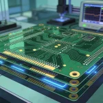
In modern electronics, Control PCBs have become an essential part of systems that require intelligent signal processing, monitoring, automation, and decision-making. Unlike conventional PCBs that primarily provide electrical connections between components, a control PCB integrates processing devices, communication interfaces, power management circuits, sensors, and input/output interfaces to control the operation of an entire electronic system.
Industrial control PCBs are widely used in industrial automation, automotive electronics, consumer electronics, medical equipment, telecommunications, IoT devices, robotics, and other advanced applications. As electronic systems become smaller, smarter, and more interconnected, control PCB designs must provide excellent signal integrity, thermal management, reliability, electromagnetic compatibility (EMC), and functional safety.
This guide explains what a control PCB is, its structure, types, design considerations, manufacturing and assembly processes, applications, advantages, challenges, and how to select a reliable control PCB manufacturer.
What Is a Control PCB?
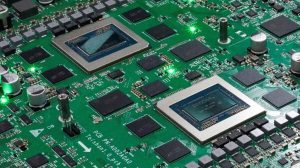
A control PCB (Control Printed Circuit Board) is a circuit board designed to monitor inputs, process information, execute control logic, and generate outputs that determine how an electronic or electromechanical system operates.
Unlike a conventional PCB that primarily provides physical and electrical interconnections between components, a control PCB typically contains active processing and control circuitry. Depending on the application, it may integrate:
- Microcontrollers (MCUs)
- Microprocessors (MPUs)
- Digital signal processors (DSPs)
- Analog-to-digital converters (ADCs)
- Digital-to-analog converters (DACs)
- Input/output (I/O) interfaces
- Communication interfaces
- Sensors and signal-conditioning circuits
- Power-management circuits
- Memory devices
- Relays, drivers, and switching devices
The primary functions of a control PCB include signal processing, data acquisition, communication, decision-making, actuator control, monitoring, and system-level automation.
For example, an industrial controller may receive temperature and pressure signals from sensors, process the data through an MCU, compare the results against programmed thresholds, and then activate motors, valves, relays, or other actuators.
In this way, the control PCB acts as the electronic control center of a larger system.
Structure of a Control PCB
A control PCB consists of several functional and physical layers. The exact architecture depends on the application, operating environment, voltage level, communication requirements, and processing complexity.
1. PCB Substrate
The substrate provides mechanical support and electrical insulation.
FR-4 is one of the most widely used materials for general-purpose control PCBs because it provides a good balance between cost, mechanical strength, electrical performance, and manufacturability.
For specialized applications, manufacturers may use:
- High-frequency laminates
- Flexible substrates
- High-Tg materials
- Polyimide
- Metal-core materials
- Ceramic substrates
Material selection should consider operating temperature, dielectric performance, mechanical stress, moisture exposure, and expected service life.
2. Copper Layers
Copper layers form the conductive network of the control PCB. They carry:
- Power
- Ground
- Digital signals
- Analog signals
- Communication signals
- Control signals
Multilayer control PCBs can use dedicated power and ground planes to improve signal integrity, power integrity, EMI performance, and thermal distribution.
3. Solder Mask
The solder mask protects exposed copper from oxidation and contamination while helping prevent unintended solder bridges during PCB assembly.
Although green is the most common solder-mask color, other colors can also be used depending on design and manufacturing requirements.
4. Silkscreen
The silkscreen provides reference designators, polarity markings, connector labels, test-point identifiers, and other information used during assembly, inspection, maintenance, and troubleshooting.
5. Microcontroller and Processing Unit
The MCU or processor is often the central control element of the board.
It executes embedded firmware, processes sensor inputs, manages communication protocols, and generates commands for external devices.
Depending on the application, a control PCB may use an MCU based on ARM, RISC-V, or other processor architectures.
6. Input/Output Interfaces
I/O circuits connect the control PCB to external sensors, actuators, switches, displays, and other systems.
Typical interfaces include:
- GPIO
- ADC/DAC
- PWM
- UART
- SPI
- I²C
- CAN
- RS-485
- Ethernet
- USB
Industrial control applications may require isolated communication interfaces to improve system safety and noise immunity.
Types of Control PCBs
Control PCBs can be categorized according to their processing architecture, circuit technology, application, and level of customization.
1. Programmable Control PCBs
Programmable control PCBs use microcontrollers, processors, programmable logic devices, or other programmable components.
Firmware can define how the board responds to different inputs and operating conditions.
These boards are widely used in:
- Industrial automation
- IoT devices
- Robotics
- Automotive systems
- Smart appliances
2. Microcontroller-Based Control PCBs
An MCU-based control PCB combines processing, memory, timers, communication interfaces, and peripheral functions into a compact architecture.
This approach is particularly suitable for embedded systems where low power consumption, compact size, and real-time control are important.
3. Analog Control PCBs
Analog control boards process continuous electrical signals.
Typical components include:
- Operational amplifiers
- Comparators
- Filters
- Voltage references
- ADCs
- DACs
Analog control circuits are commonly used for sensor conditioning, precision measurement, motor control, and power-management applications.
4. Digital Control PCBs
Digital control PCBs process information using discrete logic levels.
They may incorporate:
- Logic gates
- Counters
- Digital processors
- Memory
- Communication controllers
- Programmable logic devices
Digital architectures are particularly useful when complex algorithms, communication, and data processing are required.
5. Custom Control PCBs
A custom control PCB is designed around the exact requirements of a specific product or system.
Custom designs can integrate processing, power management, communications, sensors, and I/O into a single compact board, reducing system size and simplifying wiring.
Control PCB vs. Power PCB
Control PCBs and power PCBs may operate together but serve fundamentally different purposes.
| Feature | Control PCB | Power PCB |
|---|---|---|
| Primary purpose | Signal processing and system control | Power conversion and distribution |
| Typical voltage | Low-voltage logic and control signals | Medium- to high-voltage power circuits |
| Typical current | Usually mA to low-A ranges | Often several amps or higher |
| Main components | MCUs, sensors, ICs, communication devices | MOSFETs, IGBTs, transformers, inductors |
| Key design concerns | Signal integrity, firmware, EMC, communication | Thermal management, current capacity, isolation |
| Typical applications | Controllers, IoT, automation, automotive electronics | Power supplies, motor drives, inverters |
In many products, the two PCB types work together. A control PCB may generate PWM or gate-drive signals while a power PCB handles high-current switching and energy conversion.
Control PCB Design Guidelines
A successful control PCB design must address electrical performance, mechanical constraints, manufacturability, thermal behavior, and electromagnetic compatibility.
1. Separate Analog and Digital Circuits
Sensitive analog circuits should be separated from high-speed digital switching circuits whenever possible.
High-frequency switching nodes can generate electromagnetic noise that interferes with low-level analog signals.
Good PCB layout practices include:
- Separating sensitive analog traces from noisy switching nodes
- Avoiding unnecessary parallel routing
- Maintaining controlled return paths
- Properly partitioning functional circuit blocks
2. Use Solid Ground Planes
A continuous ground plane provides a low-impedance return path and can significantly improve signal integrity.
It also helps reduce:
- EMI
- Ground bounce
- Crosstalk
- Return-path discontinuities
For high-speed control boards, designers should avoid unnecessarily splitting reference planes underneath critical signal paths.
3. Control Trace Width and Impedance
Trace width must be selected according to current requirements, copper thickness, temperature rise, and manufacturing capabilities.
High-speed communication interfaces may also require controlled impedance.
For interfaces such as:
- USB
- Ethernet
- CAN
- LVDS
- PCIe
- RF signals
trace width, spacing, dielectric thickness, and stackup must be carefully coordinated.
4. Optimize Component Placement
Component placement should follow functional relationships.
For example:
- Decoupling capacitors should be placed close to MCU power pins.
- Crystal oscillators should be placed near the corresponding processor pins.
- High-current components should be positioned close to their loads.
- Sensitive analog components should be separated from noisy switching components.
A well-planned placement strategy reduces routing complexity and improves overall electrical performance.
5. Thermal Management
Control PCBs may contain processors, voltage regulators, power transistors, communication modules, and other heat-generating components.
Thermal management techniques include:
- Copper pours
- Thermal vias
- Large copper areas
- Heat sinks
- Thermal interface materials
- High-Tg PCB materials
- Metal-core substrates when necessary
Thermal simulation can also be used for high-power or high-temperature applications.
6. Design for Manufacturability
Design for Manufacturability (DFM) should be considered before PCB production begins.
Designers should evaluate:
- Minimum trace width
- Minimum spacing
- Drill diameter
- Annular ring
- Solder-mask clearance
- Component spacing
- Panelization
- Assembly tolerances
Early DFM analysis can prevent unnecessary redesigns and reduce manufacturing costs.
Control PCB Manufacturing Process
A professional control PCB manufacturing process typically includes the following stages.
1. Engineering Review
The manufacturer reviews Gerber files, drill files, stackup information, BOM data, fabrication drawings, and other production documentation.
Engineering checks may identify:
- Insufficient spacing
- Manufacturing-rule violations
- Incorrect drill sizes
- Stackup problems
- Impedance issues
- Component clearance problems
2. Inner-Layer Imaging
For multilayer PCBs, the inner copper layers are transferred onto copper-clad laminate using photoresist and UV exposure.
3. Etching
Unwanted copper is chemically removed, leaving the required circuit patterns.
4. Lamination
The inner layers, prepreg, and copper foils are stacked and laminated under controlled temperature and pressure.
This creates the multilayer PCB structure.
5. Drilling
CNC drilling creates:
- Through holes
- Via holes
- Component holes
- Mechanical holes
For advanced control boards, laser drilling may also be used for microvias and HDI structures.
6. Copper Plating
Copper is deposited onto hole walls to establish reliable electrical connections between PCB layers.
Proper plating thickness is particularly important for via reliability and long-term thermal cycling performance.
7. Outer-Layer Imaging and Etching
The outer copper layers are patterned and etched according to the PCB design.
8. Solder Mask and Surface Finish
The solder mask protects the copper surface, while the surface finish protects exposed pads and improves solderability.
Common finishes include:
- HASL
- Lead-free HASL
- ENIG
- ENEPIG
- OSP
- Immersion tin
ENIG is particularly common for fine-pitch components and applications requiring a flat surface.
9. Electrical and Visual Testing
Finished control PCBs can undergo:
- AOI
- Electrical testing
- Flying-probe testing
- ICT
- Functional testing
- X-ray inspection
- Impedance testing
The appropriate testing method depends on PCB complexity and production volume.
Control PCB Assembly Process
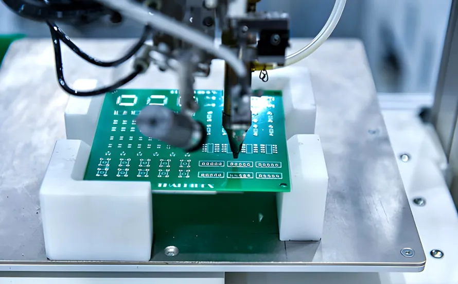
After PCB fabrication, electronic components are mounted through a professional PCB assembly process.
1. Solder Paste Printing
A stencil printer applies solder paste to the required component pads.
The accuracy of solder-paste deposition directly affects solder-joint quality.
2. Pick and Place
Automated pick-and-place machines position components onto the PCB.
Modern assembly lines can place:
- ICs
- Resistors
- Capacitors
- Connectors
- Sensors
- BGA components
- Other SMD components
3. Reflow Soldering
The assembled PCB passes through a controlled reflow oven.
The solder paste melts and forms reliable solder joints as the board moves through defined temperature zones.
4. Inspection
AOI and X-ray inspection can identify defects such as:
- Missing components
- Incorrect component orientation
- Solder bridges
- Insufficient solder
- BGA voids
- Open solder joints
5. Functional Testing
Functional testing verifies whether the assembled control PCB performs its intended functions.
For complex controllers, testing may include firmware programming, communication testing, sensor simulation, and system-level validation.
Applications of Control PCBs
Control PCBs are used across numerous industries.
Consumer Electronics
Control boards are found in:
- Smart appliances
- Home automation systems
- Wearable devices
- Smart speakers
- Consumer IoT products
They control sensors, displays, motors, wireless communication, and user interfaces.
Automotive Electronics
Automotive control PCBs are used in:
- Engine control units
- Battery management systems
- Body control modules
- Motor controllers
- Sensor modules
- Infotainment systems
Automotive applications require excellent resistance to vibration, temperature cycling, moisture, and electrical transients.
Industrial Automation
Industrial control PCBs are essential to:
- PLC systems
- Motor controllers
- Robotics
- Industrial sensors
- Factory automation
- Machine vision systems
- Process-control equipment
Industrial environments often require high EMC performance and long-term reliability.
IoT Devices
IoT control PCBs integrate processors, sensors, wireless communication, and power-management circuits.
Applications include:
- Smart gateways
- Environmental sensors
- Asset trackers
- Remote monitoring equipment
- Smart building systems
Medical Electronics
Control PCBs are also used in medical and diagnostic equipment where precise signal processing and reliable operation are critical.
Aerospace and Defense
Advanced control boards can be used in avionics, communication equipment, unmanned systems, navigation equipment, and other mission-critical electronic systems.
These applications typically require strict environmental and reliability requirements.
Advantages of Control PCBs
High Functional Integration
A control PCB can integrate processing, communication, sensing, and control functions into a single compact assembly.
This reduces wiring complexity and system size.
Improved Reliability
A properly designed PCB eliminates many unnecessary connectors and wire harnesses, reducing potential failure points.
Compact Design
Multilayer PCB technology and HDI structures allow manufacturers to integrate increasingly complex circuits into smaller form factors.
Mass Production Capability
Once the design is validated, automated PCB assembly enables consistent and scalable production.
Flexible System Control
Programmable controllers can be updated through firmware, allowing manufacturers to modify system behavior without completely redesigning the hardware.
Challenges in Control PCB Manufacturing
Despite their advantages, control PCBs also present several challenges.
Signal Noise and EMI
Industrial environments may contain motors, relays, switching power supplies, and other sources of electromagnetic interference.
Poor grounding, routing, and shielding can cause communication errors or unstable operation.
Miniaturization
As components become smaller and functionality increases, PCB layouts become increasingly dense.
Designers must carefully manage:
- Component spacing
- Thermal dissipation
- Signal integrity
- Manufacturing tolerances
- Assembly yield
Thermal Stress
Long-term operation at elevated temperatures can accelerate component aging and PCB material degradation.
High-temperature applications may require high-Tg materials, thermal vias, thicker copper, or advanced cooling structures.
Reliability Requirements
Industrial control boards may operate continuously for years.
Therefore, the design must account for:
- Thermal cycling
- Mechanical vibration
- Humidity
- Corrosion
- Electrical transients
- Component aging
How to Choose a Control PCB Manufacturer
Selecting the right control PCB manufacturer is critical to achieving reliable product performance.
Certifications and Quality Systems
Evaluate whether the manufacturer maintains relevant quality certifications and follows appropriate industry standards.
Depending on the application, these may include:
- ISO 9001
- ISO 13485
- IATF 16949
- UL
- IPC standards
Testing Capabilities
A qualified manufacturer should have appropriate testing capabilities, including:
- AOI
- X-ray inspection
- Electrical testing
- ICT
- Flying-probe testing
- Functional testing
PCB Prototyping
Prototype manufacturing allows engineers to identify design problems before committing to mass production.
A good supplier should support both prototype and volume production.
Component Sourcing
Reliable component sourcing is especially important for control PCB assembly.
A professional supplier should maintain a traceable supply chain and have effective procedures for preventing counterfeit or unauthorized components.
Engineering Support
Beyond manufacturing capacity, engineering support is valuable for DFM analysis, stackup optimization, component substitution, PCB assembly optimization, and production troubleshooting.
Future Trends in Control PCB Technology
Control PCB technology is evolving toward greater integration, higher processing capability, smaller form factors, and improved reliability.
Miniaturization Through HDI and mSAP
HDI PCB technology and modified semi-additive processing (mSAP) allow manufacturers to create finer lines, smaller vias, and higher interconnection density.
This enables increasingly compact control systems.
Flexible and Stretchable Electronics
Flexible PCB technology allows control electronics to conform to curved surfaces.
This is particularly promising for wearable electronics, medical devices, automotive interiors, and smart products.
Advanced Thermal Management
Future control PCB designs will increasingly incorporate:
- Embedded thermal structures
- Advanced copper architectures
- Ceramic substrates
- Metal-core PCB technology
- Improved thermal vias
These technologies can help control heat in high-performance electronic systems.
Edge Processing and AI
As intelligent devices become more common, control PCBs are increasingly integrating processors capable of local data analysis and AI-based decision-making.
Edge processing reduces dependence on cloud connectivity and can improve response time for real-time control applications.
Increased Functional Integration
Future control boards will combine more functions into fewer assemblies, including sensing, processing, wireless communication, power management, and security.
This trend will make high-density PCB design increasingly important.
Why Choose Kingda for Control PCB Manufacturing?
At Kingda, we focus on transforming complex PCB designs into reliable manufactured products. Our control PCB manufacturing capabilities can support demanding applications that require precise fabrication, reliable PCB assembly, and rigorous quality control.
A professional control PCB manufacturing partner should be capable of supporting customers throughout the entire product development cycle, from prototype development and DFM analysis to PCB fabrication, component sourcing, assembly, inspection, and functional testing.
Kingda can provide:
- Control PCB prototyping and mass production
- Multilayer PCB manufacturing
- PCB assembly services
- Component sourcing
- DFM engineering support
- AOI and X-ray inspection
- Electrical and functional testing
- Customized PCB solutions for industrial and electronic applications
Choosing the right manufacturing partner can reduce development risks, improve production consistency, and accelerate time to market.
Conclusion
A control PCB is much more than a conventional circuit board. It serves as the electronic control center of many modern products, integrating processing, sensing, communication, power management, and decision-making functions into a compact assembly.
From industrial automation and automotive electronics to IoT, medical equipment, and consumer electronics, control PCBs play a critical role in modern electronic systems.
A successful control PCB requires careful attention to PCB layout, signal integrity, power integrity, thermal management, EMI/EMC performance, component selection, manufacturability, and testing.
As electronic systems continue to become smaller, smarter, and more connected, technologies such as HDI, mSAP, flexible PCB, advanced thermal management, and edge computing will further expand the capabilities of control PCBs.
For companies developing sophisticated electronic products, partnering with an experienced control PCB manufacturer such as Kingda can help ensure reliable fabrication, efficient assembly, rigorous testing, and consistent long-term performance.