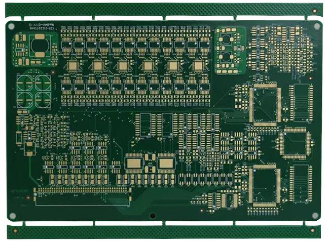
In the field of component interconnection technology for electronic products, printed circuit boards (PCBs) are widely used as the fundamental platform for connecting and supporting electronic components. With the continuous increase in the packaging density of modern electronic and electromechanical components, the requirements for printed circuit boards (PCBs) are becoming increasingly demanding. As the number of PCB layers increases, circuit traces become finer, while the overall thickness of the boards tends to decrease. Particularly over the past decade, the rapid development of integrated circuit (IC) technology has resulted in higher requirements for mounting and interconnecting integrated circuits on printed circuit boards.
To achieve the required production yield and cost efficiency, Kingda believes that certain limitations should be taken into consideration during practical operations. In addition, human factors, manufacturing capabilities, and assembly requirements should be considered before and during PCB design. These considerations can help reduce manufacturing problems and improve the reliability of the final product.
The main limitations are as follows:
- If the line spacing is less than 0.1 mm, it may be difficult to achieve a reliable etching process. This is because the etching solution cannot diffuse effectively within such a narrow space. As a result, some unwanted metal may remain between adjacent traces, which can lead to electrical shorts or other manufacturing defects.
- If the line width is less than 0.1 mm, the circuit trace may become excessively fragile during the etching process. Problems such as trace breakage, thinning, or mechanical damage may occur, thereby reducing the reliability of the PCB.
- The pad size should be at least 0.6 mm larger than the corresponding hole size. Sufficient pad area is necessary to ensure reliable component mounting and soldering. An appropriately sized pad also provides better mechanical strength and helps prevent soldering defects.
The following constraints also influence the overall PCB layout and design methodology:
- The size and performance of the camera used to reproduce the original artwork for the product;
- The dimensions and manufacturing requirements of the original artwork;
- The working dimensions of the PCB;
- Drilling accuracy and the positioning accuracy of drilled holes;
- The performance and stability of high-quality etching equipment.
These factors should be evaluated before the PCB enters mass production. A PCB design that looks feasible in design software may still encounter problems during actual manufacturing if the design exceeds the capabilities of the production equipment. Therefore, effective communication between PCB designers, engineers, and manufacturers is essential. Design-for-manufacturing considerations should be incorporated at an early stage so that potential production risks can be identified before fabrication.
PCB Design Considerations for Assembly
During PCB design, designers should also consider various parameters from the perspective of PCB assembly. The mechanical relationship between components, holes, pads, and other structures has a direct influence on assembly quality.
First, the hole diameter should be determined according to the Maximum Material Condition (MMC) and Least Material Condition (LMC). When selecting the hole diameter for an unsupported component, the MMC of the pin should be subtracted from the MMC of the hole, and the resulting difference should generally be maintained between 0.15 mm and 0.5 mm. This tolerance range provides sufficient clearance for component insertion while preventing excessive movement.
For rectangular or bar-shaped pins, the difference between the nominal diagonal dimension of the pin and the inner diameter of the unsupported hole should not exceed 0.5 mm and should not be less than 0.15 mm. Proper clearance is particularly important because insufficient clearance can make component insertion difficult, while excessive clearance may result in component movement or inaccurate positioning during PCB assembly.
Second, small components should be positioned appropriately so that they are not covered or obstructed by larger components. This is particularly important for automated assembly and subsequent inspection or maintenance. Components should be arranged so that assembly equipment has sufficient access to the required areas. Appropriate spacing also makes rework and troubleshooting easier.
Third, the thickness of the solder mask should not exceed 0.05 mm where applicable. Proper control of the solder mask helps maintain the required insulation and solderability of the PCB while preventing unnecessary interference with component mounting and solder joints.
Fourth, screen-printing markings should not overlap or intersect any pads. Clear and correctly positioned reference markings are important for component identification, assembly, inspection, and maintenance. If a marking overlaps a pad, it may interfere with soldering or make component identification more difficult.
Fifth, the upper and lower portions of the PCB structure should be designed as symmetrically as possible. Structural symmetry is important because an asymmetrical PCB may experience uneven mechanical stress during manufacturing processes involving heat. This can result in PCB warpage or bending, which may cause difficulties during component assembly and soldering. A balanced structure can therefore improve dimensional stability and production consistency.
Component Positioning and Soldering Requirements
From the perspective of PCB assembly, another important factor is the possible inclination of inserted components relative to their theoretical positions before soldering. Excessive component inclination can cause adjacent pins or solder joints to come into contact with each other, potentially resulting in short circuits or other assembly defects.
Based on practical experience, the allowable inclination of component pins should generally be maintained within approximately 15 degrees of their theoretical positions. When there is a relatively large difference between the diameter of the hole and pin, the inclination angle may reach approximately 20 degrees. For vertically mounted components, the inclination may reach 25 or even 30 degrees. However, excessive inclination reduces the effective component packaging density and may also make automatic assembly, inspection, and maintenance more difficult.
Therefore, the mechanical arrangement of components should be considered together with their electrical and thermal requirements. Sufficient clearance should be provided between components, especially for high-power or high-temperature components. Proper component spacing can also improve heat dissipation and reduce the risk of thermal interference. For sensitive components, the layout should also take into account potential mechanical stress, electrical interference, and the requirements of the final product enclosure.
Maintainability of Multiple PCB Assemblies
The use of multiple circuit boards in a single electronic product can make field maintenance and repair more convenient. Instead of disassembling the entire product, technicians can remove an individual PCB and replace it with a new one. This approach can significantly reduce maintenance time and simplify troubleshooting.
However, this method is practical only when each independent circuit board can perform a relatively unique and complete function. If several boards are highly dependent on one another, replacing a single board may still require extensive disassembly and additional repair work. Therefore, modular design should be considered during the PCB development process.
A modular PCB structure can also reduce the number of soldering and desoldering operations required during maintenance. Fewer soldering operations not only save labor time but also reduce the possibility of damaging components or PCB pads. Consequently, maintainability should be regarded as an important design objective in addition to electrical performance and manufacturing cost. Convenient access to connectors, test points, and serviceable components can further improve field maintenance efficiency.
Influence of Soldering Equipment on PCB Design
The soldering technologies and equipment used during the assembly process also impose many restrictions on PCB design and layout. Designers must understand the actual capabilities and limitations of the assembly equipment before finalizing the PCB design.
For example, in wave soldering, the size of the soldering bath, the distance between PCB edges, the component layout, and the available operating space are all important considerations. Components that are unsuitable for wave soldering may require special protection or alternative assembly methods. The direction in which the PCB passes through the equipment and the location of components relative to the solder flow can also affect soldering quality.
At the same time, PCB designers should understand the structure and appearance of the finished product as thoroughly as possible. Sensitive components should be positioned carefully and protected against possible mechanical or environmental damage. For example, high-voltage circuits should be adequately insulated and protected from unintended contact with the external environment.
The circuit boards and components inside the final product should also be arranged carefully to prevent damage caused by external objects, vibration, mechanical stress, or improper handling. Appropriate clearances, protective structures, and mechanical supports can improve the overall reliability and service life of the electronic product.
In conclusion, modern PCB design is not limited to electrical circuit design alone. It requires comprehensive consideration of manufacturing technology, PCB assembly, component placement, soldering processes, mechanical structure, maintainiablity, reliability, and production cost. By taking these factors into account at the early design stage, Kingda can help reduce manufacturing defects, improve production efficiency, and achieve higher product quality. A well-designed PCB should therefore balance electrical performance with manufacturability and assembly requirements, ensuring that the final electronic product can be produced efficiently, maintained conveniently, and operated reliably over its intended service life.