Electric Vehicle PCB Manufacturing: Complete Guide to Standards, Materials, and Process
Electric vehicle PCB manufacturing demands circuit boards that withstand extreme thermal cycling, high voltage, and vibration while maintaining reliability for 15+ years. The global PCB for electric vehicles market is expected to reach USD 24.7 billion by 2033, growing at 16.2% CAGR as EV adoption accelerates[reference:0][reference:1]. This guide covers the essential standards, materials, and manufacturing processes for EV-grade PCBs.
What Makes Electric Vehicle PCBs Different from Standard Boards?
Electric vehicle PCBs operate in environments far harsher than consumer electronics. Unlike standard FR-4 boards, EV PCBs must handle sustained temperatures above 125°C in under-hood applications, with powertrain-adjacent electronics reaching 150°C[reference:2]. A modern electric vehicle contains over 3,000 semiconductor chips and requires PCBs that support 400V to 800V battery systems, high-current power conversion, and high-speed data for ADAS and autonomous driving[reference:3]. The PCB content in a battery-electric vehicle is roughly double that of an internal combustion engine vehicle, with an estimated USD 150–200 worth of PCBs across inverters, chargers, and battery management units[reference:4].
EV PCBs must comply with a layered system of standards: bare-board qualification (IPC-6012 and its automotive addendum), component qualification (AEC-Q series), and quality management frameworks (IATF 16949)[reference:5]. None of these alone makes a board road-ready — engineers must address all three.
Key Standards for Electric Vehicle PCB Manufacturing
IPC-6012F Class 3/A: The New Automotive Reliability Benchmark
The IPC officially released IPC-6012F in Q1 2026, representing the most significant tightening of automotive PCB reliability requirements in over a decade[reference:6]. For Class 3/A automotive boards, IPC-6012F introduces several critical changes:
| Requirement | IPC-6012E Class 3/A | IPC-6012F Class 3/A | Unit |
|---|---|---|---|
| Via resistance change after thermal cycling | ≤ 10% | ≤ 5% | % |
| Plated through-hole copper thickness (barrel) | 25 | 28 | µm |
| IST cycles to failure (minimum) | 500 | 1000+ | cycles |
| Thermal shock cycles | 100 | 500 | cycles |
Source: IPC-6012F automotive addendum requirements[reference:7][reference:8]
The standard also requires stacked micro-vias (common in HDI designs for radar and lidar controllers) to be qualified at the stack level, not just the single-via level — addressing a failure mode where stacked structures passed single-via testing but exhibited delamination under extended thermal cycling[reference:9].
IATF 16949 and AEC-Q Requirements
EV PCB manufacturers must maintain IATF 16949 certification, which requires statistical process control (SPC) for critical dimensions, Production Part Approval Process (PPAP) for every new design, Failure Mode and Effects Analysis (FMEA) for manufacturing processes, and complete traceability from raw materials to finished boards[reference:10]. All components must pass AEC-Q100 (active components) or AEC-Q200 (passive components) certification[reference:11]. AEC-Q200 is often confused with a PCB standard, but it specifically qualifies passive components — resistors, capacitors, inductors — that are soldered onto the board[reference:12].
High-Voltage Insulation: Creepage and Clearance
EV PCBs operating at 400–800V require careful creepage and clearance design to prevent arcing and insulation breakdown[reference:13]. At 800V working voltage, Pollution Degree 2, and standard FR-4 (Material Group IIIa), IEC 60664-1 calls for approximately 8 mm of creepage between high-voltage and low-voltage domains[reference:14][reference:15]. For voltages over 250V, PCB designers use cutouts (grooves or notches) to improve creepage distances between conductive paths[reference:16].
PCB Materials for Electric Vehicle Applications
High-Tg Laminates: Thermal Stability Under Extreme Conditions
Standard FR-4 is inadequate for EV applications. High-Tg materials maintain mechanical modulus at elevated temperatures, protecting solder joints and microvias from fatigue. Key automotive-grade materials include:
- Nanya NPG-220: Ultra-high-Tg (220°C DMA) halogen-free material with Z-axis CTE of 30–35 ppm/°C, ideal for Grade 0 and Grade 1 automotive applications[reference:17][reference:18]
- Nanya NPG-181PY: High-Tg (180°C TMA) material with CTI 600V rating, optimized for ADAS and high-voltage EV power electronics[reference:19][reference:20]
- Isola IS420 and Panasonic R-1566W: Competing high-Tg laminates for EV and ADAS boards[reference:21]
For automotive applications, IPC-6012F requires Tg ≥ 180°C (many projects now specify ≥ 200°C), Td ≥ 360°C, CTI ≥ 600V for high-voltage isolation, and low Z-axis CTE[reference:22].
Heavy Copper for High-Current Handling
EV power electronics — traction inverters, DC-DC converters, and battery management systems — widely utilize heavy copper PCBs with 2–5 oz copper thickness to enable high-current handling[reference:23][reference:24]. For extreme applications, some designs require up to 10 oz copper[reference:25]. Heavy copper PCBs reduce resistive losses and improve thermal dissipation in high-power circuits.
Low-Loss RF Materials for Radar and Communication
77 GHz automotive radar modules require specialized low-loss RF substrates with dielectric constant (Dk) tolerance of ±2%, dissipation factor (Df) < 0.004 at 77 GHz, thickness tolerance of ±5%, and very low profile (VLP) copper foil[reference:26]. Rogers and other PTFE-based laminates are commonly specified for these high-frequency applications[reference:27].
Types of PCBs Used in Electric Vehicles
Different EV subsystems require different PCB technologies based on electrical, thermal, and packaging requirements[reference:28]:
| EV Subsystem | PCB Type | Key Benefits |
|---|---|---|
| Battery Management System (BMS) | Multilayer HDI + IMS hybrid | Dense sensing circuits, high-voltage isolation, excellent thermal management[reference:29] |
| Traction Inverter | Insulated Metal Substrate (IMS) | Superior thermal dissipation, high-current handling[reference:30] |
| DC-DC Converter | Multilayer power board | EMI suppression, efficient thermal performance, voltage regulation[reference:31] |
| Motor Drive Control | Heavy copper multilayer | Current-carrying capacity, power integrity, thermal reliability[reference:32] |
| ADAS / Radar | HDI with low-loss RF materials | High-frequency signal integrity, compact form factor[reference:33] |
| Power Distribution Unit | Heavy copper | High-current distribution, electrical fault protection[reference:34] |
Thermal Management in Electric Vehicle PCBs
Why Standard PCBs Fail at High Power
FR-4 has a thermal conductivity of just 0.3 W/m·K — excellent as an electrical insulator but terrible as a thermal conductor[reference:35]. For components dissipating less than 5W, thermal vias provide adequate heat removal. But as power density increases — 30W LEDs, 50W GaN amplifiers, 200W motor drivers — the thermal resistance through FR-4 becomes the dominant bottleneck[reference:36].
Copper Coin Technology
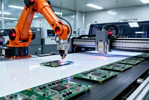
Copper coin technology replaces the FR-4 dielectric directly beneath the heat source with solid copper (thermal conductivity of 400 W/m·K), creating a thermal superhighway from junction to heatsink[reference:37][reference:38]. This provides approximately 1000× thermal conductivity improvement over FR-4 while maintaining the routing density of a standard multilayer PCB — something aluminum-core (IMS) boards cannot offer due to their single or double-layer routing limitation[reference:39].
Additional Thermal Management Strategies
EV power boards employ multiple thermal management techniques: thermal vias under components to transfer heat to inner or backside planes, large copper pours for heat dissipation, thick core substrates for mechanical and thermal stability, and proper placement of heatsinks and thermal pads[reference:40]. Thermal simulation early in the design cycle helps identify and mitigate hotspots[reference:41].
Manufacturing Challenges for Electric Vehicle PCBs
CTE Mismatch and Via Reliability
Copper has a CTE of approximately 17 ppm/°C, while FR-4 has in-plane CTE of ~14 ppm/°C and Z-axis CTE of ~50 ppm/°C[reference:42]. This mismatch creates mechanical stress on plated through-hole vias during thermal cycling. High-Tg materials with low Z-axis CTE (such as NPG-220 at 30–35 ppm/°C) minimize this stress[reference:43].
PCB Warpage in Large Power Boards
Large power boards are prone to warpage due to uneven copper balance, thermal stress from large MOSFETs and busbars, and asymmetric stack-ups[reference:44]. Controlled lamination with symmetric stack-up design improves flatness and prevents reflow issues for small control components[reference:45].
High-Voltage Isolation and CAF Resistance
Conductive Anodic Filament (CAF) growth is a critical failure mode in high-voltage EV PCBs. CAF occurs when copper ions migrate through the PCB substrate under high voltage and humidity, creating internal shorts[reference:46]. High-Tg materials with CAF-resistant resin systems are essential for 400–800V applications[reference:47].
Quality Assurance and Testing for EV PCBs
Automotive-grade PCBs require rigorous testing beyond standard commercial boards. The zero-defect expectation for safety-critical boards targets defect rates below 50 DPPM (defective parts per million), with some programs requiring < 10 DPPM[reference:48]. 100% automated optical inspection (AOI) and automated X-ray inspection (AXI) are mandatory[reference:49]. Every board must be traceable to its specific production batch[reference:50].
Interconnect Stress Testing (IST) has become a cornerstone of PCB reliability testing for automotive applications. Under IPC-6012F, IST is no longer optional — it is a mandatory qualification requirement with significantly enhanced cycling thresholds[reference:51].
Frequently Asked Questions About Electric Vehicle PCB Manufacturing
What copper thickness is recommended for EV power PCBs?
For high-current traces in inverters and power distribution, 2–5 oz copper is commonly specified. Some extreme applications require up to 10 oz[reference:52][reference:53].
Are standard FR-4 materials sufficient for EV PCBs?
No. Standard FR-4 lacks the thermal stability, CAF resistance, and high-voltage insulation required for EV applications. High-Tg (≥ 180°C) or specialized high-temperature laminates are required[reference:54][reference:55].
What is the difference between IPC-6012DA and IPC-6012FA?
IPC-6012DA was the first automotive addendum built on IPC-6012 Revision D. IPC-6012FA is the current addendum paired with IPC-6012F (released December 2025), incorporating updated requirements for back-drilled structures, microvia reliability, and board cavities[reference:56].
How do EV PCBs handle 800V systems?
At 800V working voltage, PCBs must maintain at least 8 mm creepage (IEC 60664-1, Pollution Degree 2, FR-4 Material Group IIIa). High-CTI materials (CTI ≥ 600V), conformal coating, and proper isolation barriers are also required[reference:57][reference:58].
Summary: Key Takeaways for EV PCB Manufacturing
- Standards compliance is non-negotiable: IPC-6012F Class 3/A, IATF 16949, and AEC-Q component qualification are mandatory for automotive-grade boards[reference:59][reference:60].
- Material selection determines reliability: High-Tg laminates (≥ 180°C), low Z-axis CTE, and CAF-resistant resins are essential for EV applications[reference:61].
- Thermal management requires advanced solutions: copper coin technology, thermal vias, heavy copper planes, and IMS substrates address the high power density of EV electronics[reference:62][reference:63].
- High-voltage design demands rigorous creepage and clearance: 800V systems require ~8 mm creepage with proper isolation barriers[reference:64].
- Zero-defect quality is the expectation: < 50 DPPM, 100% AOI and AXI, and full traceability are standard requirements[reference:65].
Electric vehicle PCB manufacturing represents one of the most demanding segments of the electronics industry. As EV adoption accelerates and power densities increase, PCB manufacturers must continuously invest in advanced materials, process controls, and testing capabilities to meet the evolving requirements of automotive OEMs and Tier 1 suppliers.
Ready to start your EV PCB project? Explore our prototype PCB assembly services or low-volume production capabilities. For high-volume EV programs, our high-volume PCB assembly is built for automotive-scale production. Need a complete solution? Our turnkey PCB assembly covers everything from design to delivery.
Get a free DFM analysis for your EV PCB design — upload your Gerber files and bill of materials for a comprehensive design for manufacturability review. Our engineering team will provide detailed feedback on stack-up, material selection, and manufacturing feasibility for automotive-grade production.
References
- AtlasPCB. (2026). IPC Releases Updated IPC-6012F Standard with Stricter Reliability Requirements for Automotive PCBs.
- AtlasPCB. (2026). 汽车电子可靠性要求日趋严格:PCB制造商须应对的挑战.
- NextPCB. (2026). Automotive PCB Design: IPC-6012DA, AEC-Q200 and What Makes Car-Grade Boards Different.
- Sierra Circuits. (2026). What Kind of PCBs Power EVs?
- PCBSync. (2026). EV BMS PCB Design: Cell Monitoring, AFE, and Balancing.
- PCBSync. (2026). Nanya NPG-220: The Very High-Tg Benchmark for Next-Gen EV and ADAS PCBs.
- HTF Market Intelligence. (2026). Global PCB for Electric Vehicles Market Professional Survey Report 2026-2033.
- Topfast. (2026). Power Electronics PCB Design for EV: High Current, Thermal Management & Reliability.
- AtlasPCB. (2026). PCB Copper Coin Technology: Embedded Thermal Solutions for High-Power Applications.
- IEC. (2020). IEC 60664-1: Insulation coordination for equipment within low-voltage supply systems.