ADAS PCB Manufacturing: Complete Guide to Standards, Materials, and Production for Automotive Electronics
ADAS PCB manufacturing requires specialized substrates, precision HDI fabrication, and compliance with automotive-grade reliability standards to support 77 GHz radar, camera modules, and sensor fusion domain controllers. The global automotive PCB market is projected to reach $11.4 billion in 2026, with the ADAS segment holding the largest share at 42.59%. This guide covers everything from material selection and stackup design to assembly and quality control for ADAS PCBs.
What Is ADAS PCB Manufacturing and Why Does It Differ from Standard Automotive PCBs?
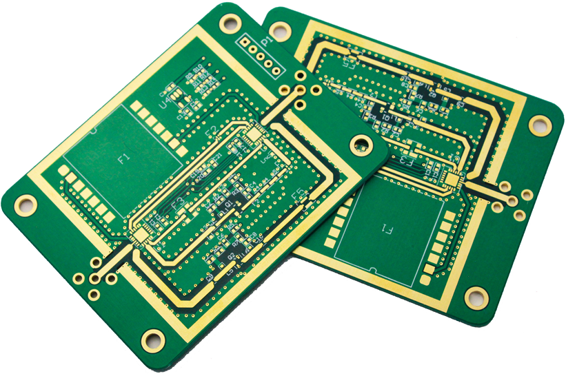
ADAS PCB manufacturing refers to the design, fabrication, and assembly of printed circuit boards used in Advanced Driver Assistance Systems—including radar modules, camera systems, lidar processors, and central domain controllers. Unlike standard automotive PCBs that operate below 1 GHz using conventional FR-4 materials, ADAS boards must handle millimeter-wave frequencies up to 81 GHz, multi-gigabit data streams, and ISO 26262 functional safety requirements.
The fundamental difference lies in three critical dimensions: frequency (77 GHz radar vs. sub-1 GHz ECUs), data rate (3–4 Gbps per camera vs. low-speed CAN buses), and safety classification (ASIL B/D vs. no functional safety requirement). These differences drive every aspect of ADAS PCB manufacturing—from material selection to layer count, plating thickness, and test protocols.
ADAS PCB Sub-Types and Their Manufacturing Requirements
ADAS electronics map to four primary PCB sub-types, each with distinct manufacturing requirements:
- Radar Module PCBs: 77 GHz millimeter-wave boards requiring low-loss RF substrates (Rogers RO3003, Taconic, AGC fastRise), controlled impedance of 50Ω single-ended, and fine-line etch capability.
- Camera Module PCBs: High-density boards with 0.4 mm pitch BGA image sensors, requiring 100Ω differential impedance (±5%) on MIPI CSI-2 lanes with matched trace lengths.
- Sensor Fusion ECU PCBs: 10–16+ layer boards combining RF, high-speed digital (DDR5, PCIe Gen4), and power domains with strict zoning and return-path discipline.
- Domain Controller PCBs: 12–20+ layer HDI boards with any-layer microvia technology for central computing platforms.
ADAS PCB Standards and Certifications: IPC-6012F, AEC-Q, and IATF 16949
ADAS PCB manufacturing is governed by a multi-layered regulatory and standards framework that ensures reliability in safety-critical automotive applications. All ADAS PCBs in production require AEC-Q100/Q200 qualified components, IATF 16949 manufacturing certification, and ISO 26262 traceability to at least ASIL B.
IPC-6012F: The New Automotive Reliability Standard (2026)
The IPC officially released IPC-6012F in Q1 2026—the most significant tightening of automotive PCB reliability requirements in over a decade. Key changes for ADAS PCB manufacturing include:
- Tighter via reliability: Resistance change reduced from 10% to 5% maximum after thermal cycling; minimum copper thickness in plated through-hole vias increased from 25 µm to 28 µm for Class 3/A.
- Stacked microvia qualification: Stacked microvias common in radar and lidar HDI designs now require individual qualification at the stack level, not just the single-via level.
- Enhanced IST requirements: Interconnect Stress Test cycles increased from 500 to 1000+ for Class 3/A boards.
- Class 3/A adoption: Thermal shock requirements increased from 100 to 500 cycles.
AEC-Q and ISO 26262 Compliance
All components on ADAS PCBs must pass AEC-Q100 (active components) and AEC-Q200 (passive components) qualification. ISO 26262 functional safety requires hardware architectural metrics—SPFM and LFM—to be met at the system level, with the PCB as part of that system. Substrate choice, layer count, plating thickness, and test-access provisions all feed into the FMEA and contribute to the ASIL rating evidence package.
ADAS PCB Material Selection: High-Frequency Laminates for 77 GHz Radar
Material selection is the most critical decision in ADAS PCB manufacturing. At 77 GHz, standard FR-4 becomes virtually unusable—its dielectric properties are too variable and too lossy to produce reliable signals. Modern automotive radar requires substrates with Dk stability within ±0.05 across the panel, Df below 0.004 at 77 GHz, and moisture absorption below 0.1%.
Rogers RO3003: The Automotive Radar Standard
Rogers RO3003 has become the de facto standard for automotive radar applications, delivering an optimal balance of performance, manufacturability, and cost:
| Parameter | RO3003 Value | RT/duroid 5880 | Standard FR-4 |
|---|---|---|---|
| Dielectric Constant (Dk) @ 77 GHz | 3.00 ±0.04 | 2.20 ±0.02 | ~4.5 (highly variable) |
| Dissipation Factor (Df) @ 77 GHz | 0.0013 | 0.0009 | >0.020 |
| Insertion Loss | 0.15 dB/cm | 0.08 dB/cm | >1.0 dB/cm |
| Thermal Coefficient of Dk | -3 ppm/°C | -240 ppm/°C | N/A |
| Manufacturing Complexity | Standard | 2–3× higher | Standard |
RO3003 delivers 0.15 dB/cm insertion loss with standard fabrication processes and survives 260°C lead-free soldering reflow cycles. RT/duroid 5880 offers lower loss (0.08 dB/cm) but poor temperature stability (-240 ppm/°C) and significantly higher manufacturing complexity.
Emerging Materials for 77 GHz Applications
AGC’s fastRise low-loss non-reinforced prepreg eliminates the “fiber weave effect”—a significant source of Dk variation at millimeter-wave frequencies where the wavelength approaches the weave pitch. At 77 GHz, the signal wavelength in the substrate is approximately 1.5–2.0 mm, close enough to typical E-glass weave patterns (1.0–1.8 mm pitch) to cause measurable Dk modulation. Non-reinforced construction eliminates this issue entirely.
Isola Astra MT77 is another ultra-low loss RF/microwave laminate offering the low loss desirable for mmWave signals. For cost-optimized designs, hybrid stackups—low-loss RF laminate on outer layers with high-Tg FR-4 on inner signal/power layers—can reduce material cost by 30–50% without compromising antenna performance.
ADAS PCB Design Rules: HDI Stackup, Impedance Control, and Signal Integrity
ADAS PCB manufacturing begins with design rules that must account for millimeter-wave frequencies, high-density interconnects, and automotive environmental demands. HDI technology is essential for radar, camera, and domain controller boards.
HDI Stackup Design for ADAS
ADAS HDI boards typically use symmetrical stackups with the basic structure “signal layer – GND layer – power layer – signal layer,” with 8 or more layers and GND layer occupancy of 30% or more recommended. Symmetrical stackups improve EMC performance and suppress board warpage. Non-symmetrical stackups can cause HDI warpage exceeding 0.7%, failing IPC-6012H Class 3 warpage tolerance of 0.5% or less.
For radar modules, recommended HDI stackups include “2+N+2” or “3+N+3” configurations optimized for microstrip antenna integration and stable RF impedance control. Domain controllers regularly require 12 to 20+ layers with blind and buried vias, via-in-pad (VIPPO), and any-layer HDI technology.
Impedance Control Requirements
ADAS HDI commonly uses 50Ω (single-ended) and 90Ω (differential) impedance targets. Impedance values depend on layer thickness, dielectric constant, and trace width, calculated per IPC-2141 (high-frequency PCB design standard). Industry data shows that when HDI impedance error exceeds ±5%, ADAS distance measurement error can expand by more than 10 cm. One automaker reported that stackup design non-conformance caused 8% impedance deviation, resulting in lane-keeping function misjudgment rates exceeding 15%.
For 77 GHz radar, etch tolerance of ±0.5 mil on L1 patches and Dk variation within ±2% across the panel are required. Automotive radar operating at 76–81 GHz pushes PCB fabrication to its limits, requiring fine-line etch capability.
Camera Module Design Considerations
ADAS camera module PCBs must maintain 100Ω differential impedance (±5%) on MIPI CSI-2 D-PHY lanes with matched trace lengths to within half the dielectric wavelength. The most critical challenge is the 0.4 mm pitch BGA image sensor, which requires reliable fan-out while maintaining controlled impedance for high-speed image transmission. Laser-drilled microvias (≈100 µm diameter) are used to route signals from BGA pads to inner routing layers.
ADAS PCB Manufacturing Processes: HDI Fabrication and mSAP Technology
ADAS PCB manufacturing requires advanced fabrication processes to achieve the fine geometries, tight tolerances, and reliability demanded by automotive applications.
HDI Fabrication for ADAS
HDI fabrication for ADAS involves sequential lamination with laser-drilled blind microvias to interconnect routing layers while maintaining the compact multilayer PCB form factor. Key process parameters include:
- Laser drilling: UV laser systems achieve 50 µm aperture processing with position accuracy of ±10 µm for ADAS HDI boards. Microvias are laser-drilled at ≤150 µm diameter with an aspect ratio held at 0.75:1—tighter than the IPC-2226 maximum of 1:1—to ensure uniform copper deposition during electroplating.
- Pulse plating: High-density current pulse technology at 20 A/dm² achieves copper layer deposition with board edge uniformity variation <8%.
- Layer-to-layer registration: Sequential lamination requires precise registration to maintain impedance control across the stackup.
mSAP: Enabling Finer Geometries for ADAS
The modified Semi-Additive Process (mSAP) is expanding beyond smartphone applications into automotive ADAS modules in 2026. mSAP enables line/space geometries of <30 µm/30 µm on PCBs—roughly 2–3× finer than conventional subtractive etching. Multiple PCB manufacturers have announced dedicated mSAP capacity for automotive ADAS and AI server hardware.
mSAP is particularly valuable for ADAS camera modules, high-frequency radar boards, and autonomous driving domain controllers, meeting automotive-grade reliability requirements. The process involves laser drilling, electroless plating, dry film application, pattern plating, strip dry film, and flash etching.
Hybrid Material Processing
ADAS radar boards often use hybrid stackups combining high-frequency materials with conventional FR-4 to reduce costs. However, PTFE-based materials (Rogers RO3003, Taconic TLY-5) require specialized processing—higher lamination temperatures and modified drilling parameters. Manufacturers must manage the different thermal expansion rates between RF laminates and FR-4 to prevent delamination.
ADAS PCB Assembly: Soldering, Inspection, and Traceability
ADAS PCB assembly requirements go far beyond standard SMT processes. All components must pass AEC-Q100/Q200 certification, and full-batch traceability is achieved through barcoding or RFID to avoid the risk of counterfeit components.
Vacuum Reflow Soldering
To meet automotive standards of <2% solder voiding (compared to the 25% industry standard), vacuum reflow is employed for ADAS assemblies. This is critical for thermal management in radar and power electronics where voiding can create hot spots and reduce reliability.
Surface Finish Selection
For RF paths, immersion silver (ImAg) or OSP is recommended to maintain conductivity and flat pad planarity for ultra-fine pitch SMT assembly. ENIG surface finish per IPC-4552B is commonly specified for ADAS computing boards.
Inspection and Quality Control
Zero-defect expectations apply to safety-critical ADAS boards: defect rate targets <50 DPPM, with some projects requiring OQL <10 DPPM. 100% automated inspection including AOI + AXI is mandatory, and every board must be traceable to specific production batches.
ADAS PCB Quality and Reliability Testing
ADAS PCB manufacturing requires comprehensive reliability testing to validate performance across the vehicle’s 15–20 year operational life.
Thermal Cycling and Environmental Testing
Automotive PCBs must survive:
- Non-powertrain: -40°C to +125°C, 1000 cycles
- Powertrain: -40°C to +150°C, 1000 cycles
- Humidity exposure: 85% RH at elevated temperatures
- Vibration stress: 10–2000 Hz random vibration per ISO 16750-3
Interconnect Stress Testing (IST)
IST has been a cornerstone of PCB reliability testing for automotive applications. Under IPC-6012F, IST is no longer optional for Class 3/A boards—it is mandatory with significantly enhanced requirements.
Electrical Testing
Class 3/A boards require 100% network testing plus impedance verification, compared to Class 3 which requires 100% network testing only.
Frequently Asked Questions About ADAS PCB Manufacturing
What materials are used for ADAS radar PCBs?
ADAS radar PCBs operating at 77 GHz use specialized high-frequency laminates such as Rogers RO3003 (Dk=3.00, Df=0.0013), Taconic TLY-5, Isola Astra MT77, or AGC fastRise. Standard FR-4 causes unacceptable insertion loss above ~2 GHz.
What is the difference between ADAS PCBs and standard automotive PCBs?
ADAS PCBs operate at millimeter-wave frequencies (77 GHz), handle multi-gigabit data rates (3–4 Gbps per camera), and must meet ISO 26262 functional safety requirements (ASIL B/D). Standard automotive PCBs operate below 1 GHz with no functional safety requirements.
What certifications are required for ADAS PCB manufacturing?
ADAS PCB manufacturers must maintain IATF 16949 certification, IPC-6012 Class 3/A capability, and ISO 26262 process documentation. All components must pass AEC-Q100 (ICs) and AEC-Q200 (passives) qualification.
What is mSAP and why is it used for ADAS PCBs?
mSAP (modified Semi-Additive Process) enables line/space geometries of <30 µm/30 µm—2–3× finer than conventional etching. It is used for ADAS camera modules, high-frequency radar boards, and domain controllers where high density and fine features are required.
How does IPC-6012F affect ADAS PCB manufacturing?
IPC-6012F (Q1 2026) tightens via reliability metrics (5% resistance change vs. 10%), increases minimum copper thickness in vias (25 µm to 28 µm), requires stack-level microvia qualification, and enhances IST requirements.
Key Takeaways for ADAS PCB Manufacturing
- Standards matter: IPC-6012F (2026) introduces stricter via reliability, IST, and Class 3/A requirements that reshape automotive PCB manufacturing.
- Material selection drives performance: Rogers RO3003 is the automotive radar standard with 0.15 dB/cm insertion loss at 77 GHz.
- HDI is essential: ADAS radar, camera, and domain controller boards require HDI with laser-drilled microvias and controlled impedance within ±5%.
- mSAP enables finer geometries: Line/space <30 µm/30 µm is achievable with mSAP, expanding into automotive ADAS in 2026.
- Zero-defect quality: Safety-critical ADAS boards target <50 DPPM with 100% AOI + AXI and full traceability.
- Market growth: The ADAS PCB segment holds 42.59% of the automotive PCB market in 2026, valued at $11.4 billion.
Expert ADAS PCB Manufacturing Solutions from GoPCB
GoPCB specializes in high-reliability PCB manufacturing for automotive ADAS applications. Our capabilities include IATF 16949-certified production, IPC-6012 Class 3/A compliance, 77 GHz radar-grade substrate processing (Rogers, Taconic, AGC), HDI with laser-drilled microvias, mSAP for fine-line geometries, and complete material traceability. Whether you need prototype PCB assembly for design validation or high-volume PCB assembly for production, our engineering team provides free DFM analysis to ensure your ADAS PCB design is manufacturable and reliable.
Get a free DFM analysis for your ADAS PCB design—upload your Gerber files and specifications. Our engineers will review your stackup, impedance control, material selection, and HDI routing to identify potential manufacturing issues before production.
Explore our full range of services: PCB manufacturing, turnkey PCB assembly, and components procurement.
References
- AtlasPCB Engineering Team. (2026). IPC Releases Updated IPC-6012F Standard with Stricter Reliability Requirements for Automotive PCBs. AtlasPCB. [Industry Report]
- PCBSync. (2026). ADAS PCB Design: Radar, Camera & Sensor Fusion Engineering Guide. PCBSync. [Industry Report]
- Lin, M. (2026). RF PCB Material Selection for Automotive Radar. AtlasPCB. [Manufacturer Data]
- PCBGOGO. (2025). Automotive Electronics High-Reliability HDI Stackup Design Guide. PCBGOGO. [Industry Report]
- Lin, M. (2026). AGC Launches Advanced RF PCB Materials for 77 GHz. AtlasPCB. [Manufacturer Data]
- AtlasPCB Engineering Team. (2026). mSAP Process Gains Traction Beyond Smartphones. AtlasPCB. [Industry Report]
- GII Research. (2026). Automotive PCB Market Size, Share, Growth and Global Industry Analysis 2026-2034. [Industry Report]
- AtlasPCB Engineering Team. (2026). Automotive Electronics Reliability Requirements. AtlasPCB. [Industry Report]