In modern electronic products, controlling electromagnetic interference (EMI) has become an essential part of PCB design. As IC switching speeds increase and signal rise times become shorter, high-frequency transient currents can generate unwanted electromagnetic radiation, crosstalk, and common-mode noise.
There are many approaches to solving EMI problems, including EMI shielding materials, filtering components, optimized grounding, and simulation-based design. However, one of the most fundamental methods is to establish an appropriate PCB Stackup and carefully manage signal, power, and return-current paths.
For Multilayer PCB Design, the relationship between signal layers, Power Plane, and Ground Plane has a direct influence on Signal Integrity, power integrity, and EMI performance. Kingda recommends considering EMI control from the early stackup and layout stages rather than attempting to correct EMI problems after PCB fabrication.
1. Power Distribution and Decoupling
Placing an appropriately sized decoupling capacitor close to an IC power pin can reduce supply voltage fluctuations and provide transient current during rapid switching. However, a single discrete capacitor cannot provide low impedance across the entire frequency range because every capacitor has parasitic resistance and inductance.
When an IC switches rapidly, transient current flows through the power distribution network. The inductance of vias, traces, and component connections can generate transient voltage spikes, which may become an important source of common-mode EMI.
A properly designed Power Plane can help solve this problem. The power and ground planes in a multilayer board provide distributed capacitance and a low-inductance current path. When the Power Plane and Ground Plane are placed close together, their distributed capacitance can supplement discrete decoupling capacitors and help stabilize high-frequency current.
The connection between the IC power pins and the decoupling network should also be as short as possible. Short connections reduce parasitic inductance and improve the effectiveness of high-frequency Decoupling.
For high-speed devices, this becomes increasingly important because faster rise times contain more high-frequency harmonic energy. Therefore, the power distribution network should be designed together with the signal routing rather than treated as a separate design task.
2. Electromagnetic Shielding Through PCB Stackup
A well-designed multilayer structure can significantly improve Electromagnetic Shielding.
From the signal-routing perspective, high-speed signal traces should preferably be placed adjacent to a continuous reference plane. From the power-distribution perspective, the Power Plane and Ground Plane should be positioned close together whenever possible.
This arrangement provides several benefits:
- Reduces the loop area of high-frequency current.
- Provides a low-inductance return path.
- Improves Signal Integrity.
- Reduces common-mode radiation.
- Helps control transmission-line impedance.
- Improves power-distribution performance.
This is one of the fundamental principles of PCB Stackup design.
The closer the signal layer is to its reference plane, the smaller the electromagnetic field and current-loop area generally become. However, the exact dielectric thickness must also consider impedance requirements, fabrication capability, material selection, and manufacturing tolerances.
3. Four-Layer PCB Design
Four-layer boards are widely used because they provide a good balance between functionality and cost. However, conventional four-layer structures can present challenges for EMI control.
A typical four-layer board may use the following structure:
- Signal
- Ground
- Power
- Signal
This arrangement provides relatively good reference-plane support for the signal layers while keeping the power and ground layers relatively close.
Another possible structure is:
- Ground
- Signal/Power
- Signal/Power
- Ground
This approach can provide better Electromagnetic Shielding because the outer layers are used as reference planes. However, the available routing area and component placement must be carefully considered.
When controlled impedance is required, designers should avoid routing high-speed traces over isolated copper islands or areas where the reference plane changes abruptly. Any discontinuity in the reference plane can force the return current to take a longer path, increasing loop inductance and potentially causing additional EMI.
4. Six-Layer PCB Design
When component density and routing requirements increase, a six-layer board can provide considerably more flexibility.
A practical six-layer PCB Stackup may use the outer layers as ground or signal layers, while the internal layers provide dedicated power, ground, and signal-routing functions.
For example, a structure such as:
- Signal
- Ground
- Signal
- Power
- Ground
- Signal
can provide a useful environment for high-speed routing. Signal layers are positioned close to reference planes, while the Power Plane and Ground Plane are paired to improve power integrity.
Another commonly considered arrangement is:
- Ground
- Signal
- Power
- Ground
- Signal
- Ground
The exact stackup should not be selected only according to the number of layers. Dielectric thickness, copper thickness, material properties, impedance targets, and fabrication capabilities must also be considered.
Kingda can evaluate these parameters during the PCB manufacturing stage to help ensure that the designed stackup can be reliably produced.
5. Ten-Layer and Higher-Layer PCB Design
As PCB complexity increases, ten-layer, twelve-layer, and higher-layer boards can provide improved routing flexibility and better control of high-speed signal environments.
A key principle in Multilayer PCB Design is to keep high-speed signal layers close to their reference planes. When a signal changes routing layers through a via, its return current must also be able to transition to the appropriate reference plane.
If the return path is interrupted, the current may need to travel around an obstruction or find another connection through a distant via. This increases the current-loop area and can negatively affect Signal Integrity and EMI performance.
Therefore, when a high-speed signal changes layers, designers should consider placing a nearby ground via where appropriate. This provides a shorter return-current transition and helps maintain a compact current loop.
6. Multiple Power Plane Design
Some complex electronic systems require multiple power rails or large current distribution networks. In these cases, several Power Plane regions or dedicated power layers may be necessary.
When two power layers carry the same supply voltage, their distribution should be designed to provide reasonably balanced current paths. Significant impedance differences between parallel power paths can result in uneven current distribution and larger transient voltages.
For systems with multiple supply voltages, designers should carefully organize the relationship between each power region and its corresponding Ground Plane.
At the same time, the stackup should maintain a mechanically and electrically balanced structure that is compatible with PCB fabrication requirements.
7. Return Path Design Is Critical
One of the most important principles in EMI Suppression is controlling the return-current path.
A high-speed signal does not travel independently through a PCB. Its return current follows a path determined largely by the electromagnetic field and the available reference plane. At high frequencies, the return current generally tends to remain close to the signal trace.
Therefore, maintaining a continuous Ground Plane beneath or adjacent to a high-speed signal can significantly reduce the current-loop area.
If a signal trace crosses a split in the reference plane, the return current may be forced to detour around the split. This can increase inductance, generate additional radiation, and create signal-integrity problems.
For this reason, avoiding unnecessary gaps, slots, and discontinuities beneath critical high-speed traces is an important PCB layout practice.
8. Routing Direction and Layer Transitions
For multilayer high-speed boards, routing direction can also affect crosstalk.
Where practical, designers can route adjacent signal layers in different dominant directions, such as horizontal routing on one layer and vertical routing on the next. This reduces long parallel coupling between adjacent layers.
However, routing direction should not be considered independently from the reference-plane structure. Maintaining a continuous return path and controlled impedance is generally more important than simply enforcing horizontal and vertical routing rules.
When a signal changes layers through a via, the transition should be evaluated for:
- Via inductance
- Return-current continuity
- Reference-plane changes
- Impedance discontinuity
- Crosstalk
- EMI radiation
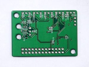
9. Copper Pour and Ground Connections
Unused PCB areas are often filled with copper to improve grounding, thermal performance, or current distribution. Properly connected copper pours can also contribute to Electromagnetic Shielding.
However, floating copper islands should generally be avoided around critical high-speed circuits because they may behave as unintended resonant structures.
Ground copper should be connected to the main Ground Plane using an appropriate number of stitching vias. Via spacing should be determined according to the highest frequency of concern, PCB geometry, manufacturing capability, and EMC requirements rather than relying on a single fixed value.
For very high-frequency applications, electromagnetic simulation can provide a more reliable basis for determining stitching-via placement.
10. PCB Stackup and EMI Control Should Be Designed Together
A successful PCB Stackup is not simply a matter of increasing the number of layers. The stackup must establish an appropriate electromagnetic environment for signal transmission and power distribution.
A well-designed structure should provide:
- Continuous reference planes for high-speed signals.
- Short and low-inductance return paths.
- Close coupling between power and ground planes.
- Controlled impedance for critical transmission lines.
- Minimal discontinuities around high-speed routing.
- Adequate isolation between sensitive and noisy circuits.
- Good manufacturability and reasonable production cost.
These factors work together to improve Signal Integrity and EMI Suppression.
Conclusion
Effective EMI control starts with PCB architecture rather than relying only on filters or shielding materials after layout completion. In Multilayer PCB Design, the relationship among the PCB Stackup, Power Plane, Ground Plane, signal routing, and return paths determines how effectively high-frequency energy is contained within the board.
As IC rise times continue to decrease, traditional layout practices may no longer provide sufficient EMI performance. Engineers should therefore consider Decoupling, impedance control, return-current paths, layer transitions, grounding, and Electromagnetic Shielding from the beginning of the design process.
Kingda combines PCB manufacturing experience with practical stackup and fabrication considerations to help customers achieve a better balance among Signal Integrity, EMI performance, reliability, manufacturability, and cost.