As electronic products become faster, smaller, and more functionally integrated, engineers face increasingly complex challenges in High-Speed PCB Design. Modern systems often combine high-speed digital circuits, sensitive analog interfaces, power management circuits, and communication modules on the same PCB. Without proper design and protection, signal noise, ground bounce, electromagnetic interference, and transient voltages can seriously affect system reliability.
For successful Mixed-Signal PCB Design, engineers need to carefully consider component placement, trace routing, grounding, power distribution, and protection components. Proper PCB Layout is particularly important because even a small amount of parasitic capacitance or inductance can significantly affect high-speed signals.
1. The Growing Challenges of High-Speed PCB Design
Modern smartphones, computers, communication systems, industrial equipment, and automotive electronics increasingly rely on system-on-chip (SoC) devices that integrate digital, analog, and power functions into a single IC.
As operating frequencies increase and supply voltages decrease, electronic devices become more sensitive to electrical disturbances. High switching currents can generate significant voltage fluctuations through PCB interconnect inductance. According to the relationship V = L × di/dt, rapid current changes can produce substantial transient voltages even across relatively short PCB traces.
Therefore, Signal Integrity and power integrity must be considered together during the design process. Poor grounding, long return paths, inappropriate trace routing, or insufficient decoupling can lead to ringing, crosstalk, ground bounce, and data errors.
2. Mixed-Signal PCB Design Requires Careful Isolation
Many modern systems combine digital and analog functions. Digital circuits typically generate fast voltage transitions, while analog circuits may process low-level signals from sensors, microphones, cameras, temperature sensors, or measurement devices.
When high-speed digital traces are routed close to sensitive analog traces, capacitive and inductive coupling can introduce unwanted noise. As PCB geometries become smaller, the distance between parallel traces decreases, increasing the possibility of parasitic coupling.
Effective Mixed-Signal PCB Design should therefore separate sensitive analog areas from noisy digital and power sections whenever possible. Engineers should also provide controlled return paths, minimize unnecessary trace crossings, and use appropriate ground and power distribution structures.
3. Why ESD and Transient Protection Are Important
Portable electronic products are frequently exposed to electrostatic discharge (ESD). A user walking across a carpet and touching a connector or enclosure can introduce a high-voltage ESD pulse into the system.
Modern ICs are often manufactured using smaller semiconductor geometries and lower operating voltages. Although these technologies provide higher performance and lower power consumption, they can also make ICs more vulnerable to electrical transients.
Effective ESD Protection and Transient Protection can redirect excessive energy away from sensitive IC pins before the voltage reaches a damaging level.
A suitable protection device should provide:
- Low capacitance for high-speed interfaces
- Fast response to transient events
- Appropriate clamping voltage
- Sufficient surge-current capability
- Low leakage current
- Compatibility with the system operating voltage
The protection component must also be selected according to the actual interface characteristics rather than simply choosing the device with the highest voltage rating.
4. TVS Diodes for High-Speed Interfaces
TVS Diodes are commonly used for ESD and transient protection in communication and data interfaces. However, conventional protection devices may introduce significant parasitic capacitance, which can degrade high-speed signal performance.
For interfaces such as Ethernet, USB, and other high-speed communication links, protection components should have sufficiently low capacitance to minimize their impact on Signal Integrity.
The selection of TVS Diodes should consider the following parameters:
- Working voltage
- Breakdown voltage
- Clamping voltage
- Junction capacitance
- Leakage current
- Peak pulse current
- ESD rating
The protection device should provide sufficient protection without creating excessive capacitive loading on the signal path.
5. PCB Layout Is Critical for Transient Protection
Component selection alone cannot guarantee effective protection. The physical PCB Layout of the protection circuit is equally important.
Fast transient currents contain high-frequency components. Even a short PCB trace can introduce parasitic inductance, which may generate additional voltage overshoot during an ESD event.
For this reason, protection components should generally be positioned as close as practical to the external connector or entry point. The path from the connector to the protection device should be short and direct, while the path from the protection device to the protected IC should also be minimized.
Designers should pay attention to:
- Connector-to-protection trace length
- Protection-to-IC trace length
- Ground return path
- Via count
- Ground-plane connection
- Trace width
- Parasitic inductance
A well-designed PCB Layout allows transient energy to be diverted before it reaches sensitive components.
6. Protecting Ethernet and USB Interfaces
Ethernet and USB are typical examples of high-speed interfaces requiring both signal integrity and protection.
For 10/100 Ethernet and higher-speed interfaces, the protection circuit must introduce minimal capacitive loading while providing effective ESD Protection. The protection components should be placed close to the connector, and the routing should maintain a controlled and predictable signal path.
USB interfaces present similar challenges. Both the high-speed data lines and power supply lines may require protection against ESD and transient events. Because USB connectors are directly accessible to users, they can become a major entry point for electrostatic discharge.
In these applications, careful component placement and low-inductance grounding are essential for effective Transient Protection.
7. Power Management and High-Current Switching
High-performance processors and communication devices can require rapidly changing current loads. When large currents switch at high speeds, the resulting voltage fluctuations can affect both power integrity and signal performance.
Modern systems therefore require efficient Power Management, including appropriate DC-DC converters, voltage regulators, decoupling capacitors, and power distribution networks.
Switching regulators improve power efficiency but can also become sources of electromagnetic noise. Designers should carefully control the high-current switching loop, minimize unnecessary copper area in noisy switching nodes, and keep sensitive analog circuits away from high-frequency power sections.
Effective Power Management should therefore be considered together with grounding, thermal management, and PCB Layout.
8. Hot-Swap and Transient Protection
Many modern systems support hot-swapping, allowing boards or peripheral devices to be inserted or removed while the system remains powered.
During insertion or removal, sudden changes in current and voltage can generate transient events. Power-management circuits should therefore incorporate suitable current limiting, soft-start, surge protection, and fault-monitoring functions.
This approach helps prevent unexpected system resets, connector arcing, and damage to sensitive components.
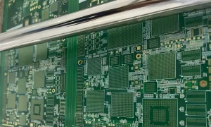
9. Key PCB Design Guidelines
To achieve reliable High-Speed PCB Design, engineers should consider the complete electrical and physical structure of the board rather than focusing only on individual components.
Key recommendations include:
- Keep high-speed signal paths short and controlled.
- Separate sensitive analog circuits from noisy digital and power circuits.
- Maintain continuous and predictable return paths.
- Minimize unnecessary vias and trace discontinuities.
- Place decoupling capacitors close to IC power pins.
- Position TVS Diodes close to external connectors.
- Minimize parasitic inductance in ESD Protection paths.
- Control impedance for high-speed interfaces.
- Keep switching power nodes away from sensitive signal traces.
- Consider thermal performance and current density during PCB Layout.
- Verify clearance, creepage, grounding, and protection requirements according to the application.
10. How Kingda Supports High-Speed PCB Manufacturing
For complex High-Speed PCB Design, manufacturing capability is closely related to final electrical performance. Trace width, spacing, dielectric thickness, layer registration, via accuracy, copper thickness, and material selection can all influence Signal Integrity.
Kingda works with customers to evaluate PCB manufacturing requirements based on operating frequency, layer structure, material selection, impedance requirements, power distribution, protection architecture, and application environment.
By combining controlled manufacturing processes with appropriate PCB Layout, grounding, ESD Protection, and Power Management strategies, Kingda helps customers develop reliable PCBs for communication equipment, industrial electronics, computing systems, automotive applications, and other high-performance products.
Conclusion
As electronic systems continue to become faster, smaller, and more integrated, High-Speed PCB Design and Mixed-Signal PCB Design require increasingly careful control of noise, power integrity, signal routing, and transient protection.
Effective Signal Integrity depends not only on high-quality ICs but also on proper PCB Layout, grounding, power distribution, TVS Diodes, and ESD Protection. At the same time, efficient Power Management is essential for controlling voltage fluctuations and minimizing switching noise.
By combining sound circuit design, optimized PCB layout, appropriate protection technologies, and reliable manufacturing processes, Kingda supports customers in achieving stable performance, improved reliability, and long-term product quality.