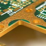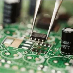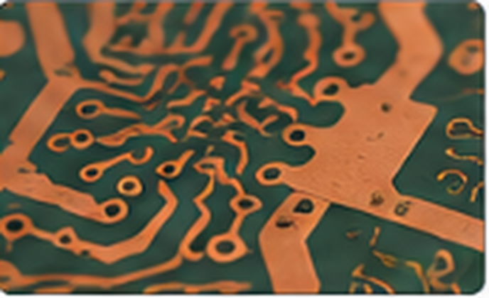
A PCB Manufacturing Process involves multiple precision-controlled steps, including circuit pattern formation, drilling, copper plating, solder mask application, surface finishing, electrical testing, and final inspection. Each stage directly affects the electrical performance, mechanical strength, solderability, and long-term reliability of the finished PCB.
According to the required circuit structure, PCBs can generally be classified into single-sided, double-sided, and multilayer boards. Although their manufacturing procedures differ, all of them require strict control of dimensional accuracy, conductor quality, insulation performance, and surface protection.
For an experienced PCB manufacturer such as Kingda, process control is not limited to individual production steps. Material selection, manufacturing tolerances, interlayer connection quality, grounding structure, and reliability requirements must be considered together to ensure that the final PCB meets both assembly and application requirements.
Single-Sided Rigid PCB Manufacturing Process
A single-sided rigid PCB generally uses a copper-clad laminate with a conductive pattern formed on one side. The basic PCB Fabrication process typically includes drilling or punching, circuit pattern formation, etching, solder mask application, legend printing, surface finishing, forming, electrical testing, inspection, and packaging.
After the copper surface is prepared, the required circuit pattern is transferred to the board using an appropriate imaging or printing process. Unwanted copper is then removed through etching, leaving the required conductive traces and pads.
A Solder Mask is subsequently applied to protect the exposed copper and reduce the risk of solder bridging during assembly. Green is the most commonly used solder mask color, although other colors such as black, blue, yellow, and red are also available depending on product requirements.
The final stages may include surface treatment, mechanical profiling, electrical open-and-short testing, visual inspection, and packaging. Proper process control at every stage helps maintain dimensional accuracy and consistent soldering performance.
Double-Sided Rigid PCB Manufacturing Process
A double-sided rigid PCB contains conductive patterns on both sides and normally requires plated through-holes to establish electrical connections between the two layers.
The manufacturing process generally includes:
- CNC drilling
- Hole inspection and deburring
- Desmear and hole-wall preparation
- Electroless copper deposition
- Pattern imaging
- Pattern plating
- Etching
- Solder mask application
- Legend printing
- Surface finishing
- Profiling and forming
- Electrical testing
- Final inspection and packaging
During the PCB Fabrication process, plated through-holes are particularly important because they provide reliable electrical interconnection between the top and bottom copper layers. Uniform copper deposition inside the hole walls is therefore essential for long-term reliability.
For higher-density designs, manufacturing tolerances must also be carefully controlled. Variations in hole position, annular ring dimensions, copper thickness, and board size can affect component assembly and electrical performance.
Multilayer PCB Manufacturing Process
The Multilayer PCB manufacturing process is developed from the double-sided plated-through-hole process but introduces additional manufacturing requirements, including inner-layer circuit fabrication, lamination, layer alignment, controlled drilling, and reliable interlayer connections.
A typical multilayer PCB process includes:
- Inner-layer circuit imaging and etching
- Inner-layer inspection and cleaning
- Inner-layer registration and alignment
- Lamination of cores and bonding materials
- CNC drilling
- Hole-wall treatment and desmear
- Electroless and electrolytic copper plating
- Outer-layer circuit formation
- Solder mask application
- Surface finishing
- Mechanical profiling
- Electrical testing and final inspection
The most important feature of a multilayer structure is the connection between different conductive layers. Plated through-holes and other interconnection structures must maintain stable electrical and mechanical performance throughout the service life of the PCB.
Layer registration is another critical factor. Even a small alignment deviation can affect vias, pads, trace spacing, and impedance-controlled structures. Therefore, Multilayer PCB production requires accurate tooling, controlled lamination parameters, and reliable inspection procedures.
The Role of Solder Mask in PCB Reliability
The Solder Mask is not simply a cosmetic layer. It plays an important role in PCB assembly and long-term protection.
During wave soldering and reflow soldering, the solder mask helps prevent solder from spreading between adjacent conductors, reducing the possibility of solder bridges and short circuits. It also protects exposed copper from moisture, oxidation, contamination, corrosion, and mechanical scratches.
A properly controlled solder mask process should provide:
- Uniform coating thickness
- Accurate registration with copper pads
- Good adhesion to the substrate
- Resistance to soldering temperatures
- Reliable insulation performance
- Stable surface appearance
For high-density PCB designs, solder mask registration becomes particularly important because the clearance between pads, traces, and mask openings can be very small.
PCB Grounding and Reliability Design
Grounding is another important part of PCB Reliability. A properly designed grounding structure can reduce noise, improve signal stability, and help control electromagnetic interference.
Electronic equipment may contain several types of reference structures, including system ground, chassis ground, digital ground, and analog ground. The appropriate grounding method should be selected according to signal frequency, circuit structure, current distribution, and system requirements.
1. Selecting Single-Point or Multipoint Grounding
For relatively low-frequency circuits, single-point grounding can help reduce unwanted ground-loop currents. As signal frequency increases, the inductive impedance of grounding conductors becomes more significant, making short and low-impedance grounding paths increasingly important.
For high-frequency designs, multipoint grounding or a continuous ground plane is often more effective because it provides shorter return paths and reduces parasitic inductance.
The transition between grounding strategies should not be based solely on one fixed frequency. PCB geometry, signal rise time, return-path structure, and operating environment should all be considered.
2. Separating Digital and Analog Circuits
When digital and analog circuits are placed on the same PCB, their physical layout should be carefully planned.
High-speed digital switching can generate transient currents and broadband noise. Sensitive analog circuits may be affected if these currents share the same return path.
Therefore, digital and analog functional areas should be appropriately separated, while their reference and return paths should be designed according to the overall system architecture. Simply splitting the ground plane without considering return-current paths can sometimes create additional impedance and EMI problems.
3. Use a Low-Impedance Ground Structure
A narrow ground trace can develop a noticeable voltage variation when carrying changing currents. This voltage fluctuation can affect logic thresholds, timing signals, analog accuracy, and overall noise immunity.
For this reason, a ground plane or sufficiently wide ground conductor is generally preferred for modern PCB designs. A continuous copper plane provides lower impedance and gives high-frequency return currents a more predictable path.
For high-speed and high-current applications, the designer should consider copper thickness, plane geometry, via distribution, current density, and thermal requirements together.
4. Ground-Loop Considerations
Ground loops can introduce unwanted circulating currents and increase susceptibility to noise. In some digital PCB structures, an appropriately designed low-impedance ground network can reduce voltage differences between different points on the board.
However, creating a closed ground path should not be treated as a universal solution. The correct approach depends on the signal frequency, current distribution, grounding architecture, and system-level EMC requirements.
For high-speed designs, maintaining a continuous reference plane and minimizing interruptions in the return-current path are generally more important than simply creating a closed copper loop.
Improving PCB Reliability Through Manufacturing Control
Good PCB Reliability depends on both design and manufacturing. Even a well-designed PCB can experience reliability problems if fabrication tolerances are not properly controlled.
Important manufacturing factors include:
- Copper thickness consistency
- Hole diameter and positional accuracy
- Plated-through-hole reliability
- Layer-to-layer registration
- Lamination quality
- Solder mask registration
- Surface finish quality
- Board thickness control
- Insulation performance
- Electrical open-and-short testing
For Multilayer PCB products, lamination and interlayer alignment require particular attention because defects inside the stack-up may not be visible during conventional visual inspection.
Kingda can evaluate PCB structure, material selection, layer count, manufacturing tolerances, electrical requirements, and assembly conditions to establish an appropriate manufacturing process for different applications.
Conclusion
A reliable PCB is the result of coordinated control across design, fabrication, assembly, and testing. From single-sided and double-sided boards to complex Multilayer PCB structures, every manufacturing stage can influence final performance.
At the same time, Grounding Design, Signal Integrity, and EMI Control should be considered during the PCB design stage rather than addressed only after manufacturing. Proper grounding, controlled return paths, suitable layer structures, and accurate fabrication can significantly improve electrical stability and product reliability.
By combining appropriate materials, precise PCB Fabrication processes, strict inspection, and application-specific reliability requirements, Kingda can help customers achieve consistent PCB quality and stable long-term performance.