2026 Any‑Layer HDI PCB Manufacturing Cost: Price Breakdown, Key Factors & Reduction Guide
As electronic devices become smaller, faster, and more functionally integrated, traditional multilayer PCBs are increasingly challenged by limited routing space. Any‑layer HDI PCB technology offers a solution by using microvias, sequential build‑up structures, and advanced interconnection techniques to enable high‑density routing across multiple layers.
However, any‑layer HDI PCB manufacturing is far more complex than standard multilayer PCB production. Laser‑drilled microvias, sequential lamination, high‑precision registration, advanced copper plating, and extra inspection steps significantly increase overall manufacturing costs.
In 2026, typical any‑layer HDI PCB fabrication prices can range from about $10 to over $150 per board, depending on board size, layer count, material, via structure, copper thickness, surface finish, production volume, and other technical requirements. For high‑volume production, the unit price can drop substantially, while prototypes and small‑batch orders typically incur higher per‑board costs.
This guide explains the major factors affecting any‑layer HDI PCB manufacturing costs in 2026 and provides practical advice for engineers, procurement teams, and OEM buyers.
1. What Is Any‑Layer HDI PCB?
With the continuous miniaturisation and higher integration of smart terminals, 5G communication, automotive electronics, medical devices, and high‑performance computing equipment, traditional multilayer PCBs are increasingly limited in routing space and interconnect density.
Any‑layer HDI PCB is an advanced PCB technology for high‑density electronic products. It uses laser microvias, sequential build‑up, fine lines, and high‑density interconnect structures to achieve more flexible and dense electrical connections between different circuit layers. This technology is often associated with ELIC (Every Layer Interconnection).
Compared with conventional through‑hole PCBs, any‑layer HDI PCBs typically employ:
- Laser‑drilled microvias
- Sequential build‑up (multiple lamination cycles)
- Fine‑line circuitry
- Small‑diameter microvias
- Via‑in‑pad
- Stacked or staggered microvias
- Copper‑filled microvias
- High‑precision copper plating
- Advanced layer‑to‑layer alignment
The core objective is to achieve higher wiring density and shorter electrical paths within a limited PCB footprint. Hence, any‑layer HDI PCBs are well suited for smartphones, wearables, 5G infrastructure, automotive electronics, medical devices, high‑end consumer electronics, industrial controls, and other high‑density applications.
Nevertheless, compared to standard multilayer PCBs, any‑layer HDI manufacturing involves more laser drilling, build‑up cycles, microvia plating, copper filling, and precision alignment steps, which drive costs significantly higher.
2. How Much Does an Any‑Layer HDI PCB Cost in 2026?
There is no single fixed price for any‑layer HDI PCBs because material, layer count, size, routing density, microvia structure, and order quantity vary greatly across projects. Based on typical 2026 market data, here are general budget ranges:
2.1 Prototype / Small‑Batch Sampling
For technically complex, low‑volume any‑layer HDI PCBs: $30–$150+ per board. If high‑speed materials, ultra‑fine lines, stacked microvias, copper‑filled vias, or special finishes are used, the price can be even higher.
For reliable prototype PCB assembly services, gopcb offers expert support for HDI projects.
2.2 Small‑Batch Production (e.g., 50–500 pieces)
Approximately $15–$80 per board, depending on size, layer count, material, microvia structure, copper thickness, finish, and quantity.
2.3 Medium‑Batch Production (500–5,000 pieces)
Roughly $10–$50 per board. As volume increases, fixed costs (engineering, CAM, tooling) are spread over more boards, reducing the unit price.
2.4 High‑Volume Production
For mature OEM volume projects: $5–$30+ per board. With optimised design, standardised materials, and large orders, unit costs can drop further.
For cost‑effective high‑volume production, explore high‑volume PCB assembly options at gopcb.
These ranges are for early budgeting only and do not replace formal quotes. Accurate pricing requires a PCB manufacturer to review Gerber files, stack‑up, material, quantity, copper weight, finish, and special requirements.
3. Main Factors Affecting Any‑Layer HDI PCB Manufacturing Cost
The final price is influenced by multiple factors, including:
- Layer count – more layers mean more material, lamination, drilling, plating, and inspection steps.
- Board size – larger sizes consume more material and may reduce panel utilisation.
- Material – standard FR‑4 is cheaper than high‑Tg, low‑loss, or high‑frequency materials.
- Microvia structure – smaller vias, higher density, and more complex stacking increase difficulty and cost.
- Number of build‑up cycles – more sequential lamination steps add material, process time, and alignment challenges.
- Copper thickness – thicker copper requires longer plating and tighter etching control.
- Surface finish – ENIG, ENEPIG, immersion silver, immersion tin, and hard gold have different costs.
- Production volume – larger volumes reduce the fixed‑cost burden per board.
- Testing and inspection – AOI, electrical test, flying probe, X‑ray, impedance testing, etc.
- Manufacturing yield – complex designs have higher defect risks; lower yields increase effective cost.
4. How PCB Material Affects Any‑Layer HDI PCB Price
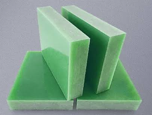
Material choice is a key cost driver. For general electronics without extreme signal speed, temperature, or reliability demands, high‑quality FR‑4 offers a good balance of performance and cost. However, high‑speed, high‑frequency, or high‑reliability products may require high‑Tg FR‑4, low‑loss materials, ultra‑low‑loss materials, high‑frequency laminates, low‑CTE materials, or specialised HDI build‑up dielectrics. For example, a high‑Tg FR‑4 any‑layer HDI board will have lower material cost than one using premium low‑loss materials for telecom applications. The right material should be selected based on actual electrical, thermal, and reliability requirements, not simply the most expensive option.
5. Impact of Layer Count and Stack‑up on Cost
Layer count is a major price factor. Common any‑layer HDI boards range from 8, 10, 12, 14, 16, to 20+ layers. Higher layer counts increase complexity—a 10‑layer board may need fewer build‑up steps, while a 16‑layer board with multiple build‑up cycles, stacked microvias, and copper‑filled vias can be significantly more expensive. More layers mean more core material, copper foil, dielectric, lamination cycles, drilling, laser drilling, tighter alignment, more complex plating, and stricter QC. Therefore, optimising the stack‑up to meet routing, electrical, and mechanical needs without over‑engineering is a key cost‑control measure.
6. Microvia and ELIC Technology Cost Impact
Microvias are central to any‑layer HDI manufacturing. Laser drilling creates very small interconnections in build‑up dielectrics, enabling high‑density layer‑to‑layer connections. Compared to mechanical drilling, laser drilling demands more advanced equipment and tighter process control. The following design choices increase costs:
- Smaller microvia diameters
- Higher microvia density
- Stacked microvias
- Staggered microvias
- Via‑in‑pad
- Copper‑filled microvias
- Multi‑layer continuous microvia interconnections
- High‑density ELIC structures
A well‑designed staggered microvia layout is generally easier to manufacture than complex stacked structures, while still meeting electrical performance. Thus, microvia design is a decisive factor in any‑layer HDI pricing.
7. Why Sequential Build‑Up Increases Manufacturing Cost
Sequential build‑up is the core process for any‑layer HDI. Unlike standard multilayer PCBs that are laminated all at once, any‑layer HDI requires multiple build‑up cycles to gradually add dielectric and copper layers, with microvias formed at each stage. A typical process includes inner‑layer circuit formation, core lamination, laser drilling, electroless copper deposition, pattern plating, build‑up dielectric application, further laser drilling, microvia plating, copper filling, sequential pressing, outer‑layer circuit formation, surface finish, AOI, and electrical testing. Each additional build‑up cycle increases material, pressing, laser drilling, plating, process time, alignment difficulty, and manufacturing risk. Therefore, optimising the stack‑up and build‑up count is essential for cost reduction.
8. Copper Plating and Surface Finish Influence on Price
Copper plating is critical for reliable microvia connections. Processes may include electroless copper, pattern plating, microvia plating, copper filling, leveling, and outer‑layer plating. Surface finish also affects cost:
- ENIG (Electroless Nickel Immersion Gold) – common for fine‑pitch devices, offers good flatness and solderability.
- ENEPIG (Electroless Nickel Electroless Palladium Immersion Gold) – adds a palladium layer, higher cost, suitable for high‑reliability and wire‑bonding applications.
- Immersion Silver – good flatness for some high‑density designs.
- Hard Gold – used for edge connectors and contacts requiring wear resistance, not for standard pads.
Specify the required finish early in the quoting process.
9. PCB Size and Design Complexity
Board size affects material usage and panel utilisation, but it is not the sole determinant. A small board with extremely high routing density can cost more than a larger but simpler multilayer board. For example, two 10‑layer boards of the same size can have vastly different costs if one uses low‑loss material, stacked microvias, via‑in‑pad, copper filling, ultra‑fine lines, fine‑pitch BGA, and tight impedance control. Thus, cost evaluation must consider the entire manufacturing structure, not just size and layer count.
10. How Production Quantity Affects Unit Price
Volume has a direct impact on unit cost. Fixed costs such as engineering review, CAM processing, setup, laser tooling, test fixtures, first‑article inspection, and parameter tuning are spread over the total number of boards. For 10 pieces, the fixed cost per board is high; for 10,000 pieces, it becomes negligible. Therefore, as quantity increases, the unit manufacturing cost decreases. OEM buyers should request quotes for multiple volumes (e.g., 10, 50, 100, 500, 1k, 5k, 10k) to understand the pricing curve. For small‑batch needs, check low‑volume PCB assembly services at gopcb.
11. Prototype vs. Volume Production Price Differences
Prototype and production prices differ significantly. Prototypes incur engineering review, DFM analysis, CAM generation, special process setup, lower panel utilisation, small‑batch equipment tuning, and extra inspection costs. A complex any‑layer HDI prototype may easily exceed $50–$100 per board. In stable volume production, unit costs drop through higher panel utilisation, optimised parameters, re‑use of engineering data, stable processes, better equipment utilisation, and improved yields. A board that costs $80 as a prototype may become much cheaper in mature volume production.
12. Testing and Quality Inspection Costs
Due to complex structures and high density, even minor defects can affect reliability. Depending on the application, manufacturers may employ AOI, electrical testing, flying‑probe, X‑ray inspection, cross‑sectioning, solderability tests, impedance tests, dimensional checks, and reliability tests. Automotive, medical, aerospace, and industrial controls often require additional validation. While testing adds cost, it prevents defective boards from entering SMT assembly and final products, saving overall expenses.
13. How to Reduce Any‑Layer HDI PCB Manufacturing Costs
Cost reduction does not mean simply choosing cheaper materials. More effective is DFM (Design for Manufacturing) optimisation from the design stage:
- Optimise the stack‑up – use a reasonable, simple layer structure; avoid unnecessary build‑up cycles.
- Simplify microvia design – if standard microvias meet requirements, avoid complex stacked structures.
- Improve panel utilisation – optimise board outline and panel layout to fit more units per panel, reducing material waste.
- Select materials based on actual needs – only use premium low‑loss materials when signal integrity, frequency, temperature, or reliability truly demand them.
- Avoid over‑specifying tolerances – extremely tight line/space, hole size, and dimensional tolerances increase difficulty. Specify practical tolerances.
- Choose a reasonable surface finish – ENIG is sufficient for most fine‑pitch soldering; ENEPIG is only needed for extra reliability or wire bonding.
- Increase production volume – consolidate orders or plan for higher quantities to reduce fixed‑cost allocation.
14. gopcb Provides Any‑Layer HDI PCB Manufacturing Services
For OEMs, ODMs, and R&D companies requiring high‑density interconnect technology, choosing a manufacturer with proven HDI capabilities is critical. gopcb offers comprehensive PCB solutions covering any‑layer HDI, multilayer, high‑speed, fine‑pitch BGA, microvia, via‑in‑pad, high‑Tg, and high‑frequency boards. For complex any‑layer HDI projects, provide complete manufacturing data: Gerber files, NC drill files, stack‑up information, board size, layer count, inner/outer copper weights, material type, surface finish, solder mask colour, quantity, electrical test requirements, impedance control, and special reliability needs. Only with full data can the manufacturer accurately assess difficulty and cost.
To reduce costs, engage gopcb early for DFM review – this avoids later cost increases due to process complexity. Learn more about our PCB manufacturing capabilities.
15. FAQ – Any‑Layer HDI PCB
1. How much does an any‑layer HDI PCB cost in 2026?
Typically $10–$150+ per board, depending on layer count, size, material, microvia structure, copper thickness, finish, testing, and volume. High‑volume production significantly lowers the unit price.
2. Why are any‑layer HDI PCBs expensive?
They require laser drilling, sequential build‑up, microvia plating, copper filling, and high‑precision alignment – much more complex than standard multilayer PCBs.
3. Is any‑layer HDI more expensive than standard HDI?
Generally, yes, because it offers more flexible interconnections and may involve more microvias and build‑up cycles. However, the final price depends on the specific design.
4. What factors influence the price most?
Layer count, material, board size, microvia structure, number of build‑up cycles, copper thickness, surface finish, manufacturing tolerances, and production volume.
5. Can any‑layer HDI costs be reduced?
Yes – by optimising stack‑up, simplifying microvia structures, improving panel utilisation, choosing suitable materials, avoiding overly tight tolerances, and increasing order quantity.
6. Is any‑layer HDI suitable for high‑speed PCBs?
Yes, it provides higher routing density and shorter interconnects, which benefit high‑speed designs. But attention must still be paid to material Dk/Df, impedance control, signal integrity, power integrity, stack‑up, trace length, return path, and copper roughness. Using any‑layer HDI does not automatically guarantee high‑speed performance.
16. Conclusion: How to Evaluate Any‑Layer HDI PCB Cost in 2026
2026 any‑layer HDI PCB manufacturing cost is not determined solely by area and layer count – the entire manufacturing structure matters. For budgeting, complex any‑layer HDI boards may range from $10 to over $150 per board, but stable high‑volume production can significantly reduce the unit price. For OEM customers, the best way to control cost is not to squeeze supplier quotes but to perform DFM optimisation early in the design phase. By optimising stack‑up, microvia structure, material, line/space, panelisation, surface finish, and production quantity, you can achieve the required electrical performance and reliability at a lower manufacturing cost.
For smartphones, 5G equipment, automotive electronics, medical devices, wearables, and other high‑density products, partnering with an experienced any‑layer HDI manufacturer like gopcb helps balance performance, reliability, yield, and cost. Contact gopcb for a feasibility review and quote based on your Gerber files, stack‑up, material, microvia structure, surface finish, and quantity.