PCB Electroless Copper vs. Electrolytic Copper Plating: Key Differences, Process Flow & Quality Control
In PCB manufacturing, copper is the most essential conductive material. Traces, pads, vias, and interlayer interconnect structures all rely on copper layers for stable electrical connections. Terms like PCB electroless copper, electrolytic plating, copper deposition, and copper plating are often used interchangeably, which can lead to confusion about process steps, copper thickness requirements, and product reliability.
So, what exactly is the difference between PCB electroless copper deposition and electrolytic copper plating?
Simply put: Copper deposition is a broader term describing the formation of a copper layer on a PCB substrate, while copper plating typically refers to processes (electroless or electrolytic) that increase copper thickness. In conventional PCB fabrication, electroless copper is used to create an initial conductive layer on non-conductive surfaces (e.g., hole walls), and electrolytic plating then builds up the required copper thickness. The two are often used sequentially.
This guide explains the definitions, process flows, applications, thickness control, common defects, and quality considerations for both processes, helping engineers and procurement professionals understand the differences.
1. What Is PCB Electroless Copper Deposition?
PCB electroless copper deposition (also known as electroless copper plating) is a critical process that forms a continuous, uniform copper layer on the PCB surface, especially on the walls of drilled holes. After drilling, hole walls are typically made of resin and glass fibers, which are non-conductive. Before subsequent electrolytic plating, the hole walls must be made conductive through electroless copper deposition.
This process is widely used for through‑hole PCBs, multilayer boards, HDI boards, flexible and rigid‑flex PCBs, automotive and industrial PCBs, and power boards. The most common method is electroless copper plating, which uses a chemical reduction reaction (without external current) to deposit a very thin copper layer on activated surfaces. This initial layer is not the final copper thickness; it provides the conductive foundation for subsequent electrolytic plating.
2. What Is PCB Copper Deposition?
Copper deposition is a broader technical concept than “plating.” It encompasses any process that deposits or forms copper material on a PCB substrate. In addition to electroless and electrolytic plating, it can include direct metallization, physical vapor deposition (PVD), chemical vapor deposition (CVD), and other specialty techniques. However, for conventional PCBs, the most common deposition methods are electroless copper followed by electrolytic copper plating. Thus, copper deposition is the overarching category, and copper plating is one of its primary implementation methods.
3. Electroless Copper vs. Electrolytic Copper Plating – The Core Differences
This is a frequent point of confusion in PCB manufacturing.
Electroless Copper Deposition:
- Requires no external electrical current.
- Uses chemical reduction reactions.
- Deposits a thin, uniform copper layer (typically 0.5–1.5 µm).
- Can coat non‑conductive surfaces (resin, glass).
- Primarily used for hole wall metallization to create a conductive base.
Electrolytic Copper Plating:
- Requires an external DC power supply.
- Relies on current density and electroplating solution.
- Rapidly builds copper thickness (to 1 oz, 2 oz, or more).
- Applied to already conductive surfaces (traces, pads, and hole walls).
- Meets final thickness, current‑carrying, and mechanical requirements.
In essence, electroless copper solves the problem of “making non‑conductive surfaces conductive,” while electrolytic plating solves “achieving the required final copper thickness.” They are complementary, not interchangeable.
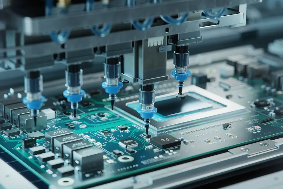
4. PCB Electroless Copper Process Flow
A typical electroless copper sequence includes:
- Drilling – mechanical or laser drilling per Gerber data.
- Deburr and desmear – remove resin smear and contaminants from hole walls.
- Conditioning and cleaning – prepare hole surfaces for activation.
- Activation – apply a catalyst (e.g., palladium) to promote the reduction reaction.
- Acceleration – enhance catalytic activity.
- Electroless copper deposition – chemical reduction deposits a thin copper layer (typically 0.5–1.5 µm).
- Electrolytic copper plating – builds up thickness to the required level.
Different manufacturers may use proprietary chemistries and parameters, but the core steps remain similar.
5. PCB Electrolytic Copper Plating
Electrolytic copper plating uses an external current to increase copper thickness. In a typical system, the PCB acts as the cathode, copper anodes supply copper ions, and the plating bath contains copper sulfate and sulfuric acid. Key control parameters include current density, plating time, copper ion concentration, acid concentration, temperature, agitation, additive levels, and anode condition. Improper control can lead to uneven thickness, voids, roughness, burning, or brittle deposits. For reliable results, precise process control is essential.
6. Why Is Electroless Copper Deposition Necessary?
Electroless copper is not just about adding a little copper; it is fundamental to reliable conductive interconnections.
- Through‑hole connectivity – for multilayer PCBs, vias connect different copper layers; electroless copper provides the initial conductive film.
- Via reliability – copper layers must withstand thermal cycling, mechanical stress, and soldering shocks.
- Current‑carrying capacity – thicker copper handles higher currents (e.g., power modules, EV chargers, motor drives).
- Mechanical robustness – good hole‑wall copper reduces crack risks during thermal cycles.
For high‑aspect‑ratio holes and HDI microvias, uniform electroless copper coverage is especially critical.
7. Common Defects and Troubleshooting
Several defects can occur if process parameters are not well controlled:
- Uneven copper thickness – caused by improper current density, poor solution circulation, or edge effects.
- Plating voids in holes – due to insufficient cleaning, desmear, activation, or solution access. Voids can cause open circuits.
- Copper peeling – from poor surface preparation, contamination, or weak adhesion.
- Rough or nodular surfaces – from high current density, bath contamination, or additive imbalance.
- Burning – localized over‑plating due to excessive current density, leading to discoloured or brittle deposits.
Regular monitoring of chemical concentrations, current distribution, and test coupons is essential to prevent these issues.
8. Choosing the Right Copper Deposition Process
Different PCBs require different approaches. Consider:
- Layer count – multilayer boards need robust hole metallization.
- Board type – HDI, flexible, rigid‑flex, heavy‑copper, and standard FR‑4 have varied requirements.
- Final copper thickness – heavier copper (3 oz, 4 oz, 6 oz) requires longer plating times and higher current.
- Via structure – microvias and high‑aspect‑ratio holes demand superior solution penetration.
- Reliability needs – automotive, medical, and aerospace applications require stricter controls and testing.
9. What Is the Typical PCB Copper Thickness?
Copper thickness is usually specified in ounces (oz) per square foot. Common values: 0.5 oz, 1 oz, 2 oz, 3 oz, 4 oz, and 6 oz or more. For standard products, 1 oz and 2 oz are typical. Heavy‑copper PCBs (≥3 oz) are used for high‑current applications. Note that base copper (starting foil) and finished copper (after plating) differ – the plated thickness adds to the base. Always specify base copper, finished copper, surface copper, and hole‑wall copper thickness in your requirements.
10. Why Multilayer PCBs Rely on Electroless Copper
Multilayer PCBs have inner copper layers separated by dielectrics. To interconnect layers, through‑holes, blind vias, buried vias, and microvias are used. Electroless copper must ensure:
- Continuous hole‑wall coverage
- Sufficient thickness
- Good adhesion
- No voids
- Thermal reliability
- Stable electrical connections
For high‑aspect‑ratio holes, the plating solution must penetrate deeply and deposit evenly. As line/space dimensions shrink, process control becomes even more critical.
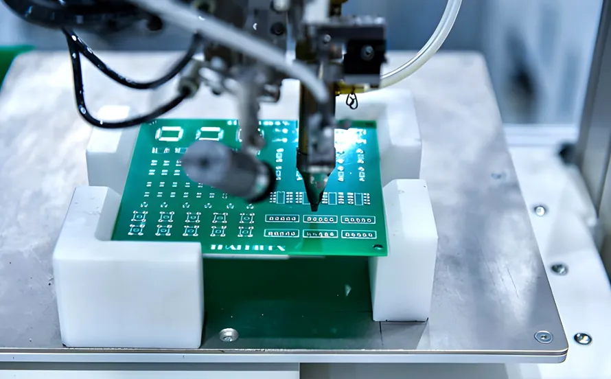
11. How gopcb Controls Electroless and Electrolytic Copper Quality
At gopcb, we understand that consistent copper deposition is the backbone of reliable PCBs. Our process controls include:
- Precise chemical bath monitoring (copper ion, reducing agents, stabilisers)
- Current density and plating time optimisation
- Temperature and agitation control
- Regular additive replenishment
- Anode maintenance and solution filtration
- Cross‑section analysis and micro‑sectioning for hole‑wall thickness
- Automated optical inspection (AOI) and electrical testing
For your project, we recommend providing detailed specifications: layer count, material, base copper, finished copper, minimum hole size, aspect ratio, via type, trace width, current requirements, and reliability class. This allows us to tailor the deposition and plating process to your needs.
Explore our PCB manufacturing capabilities and prototype assembly services for your next project.
12. Frequently Asked Questions
1. Are electroless copper and electrolytic copper the same?
No. Electroless copper uses chemical reduction without current to form an initial layer on non‑conductive surfaces. Electrolytic plating uses external current to build thickness on conductive surfaces. They are sequential steps.
2. Why can’t we just use electrolytic plating directly?
Because drilled hole walls are non‑conductive (resin/glass). Electrolytic plating requires a conductive surface to start. Electroless copper provides that conductive base.
3. What causes plating voids in holes?
Insufficient desmear, poor activation, contamination, or inadequate solution circulation can lead to voids. Proper pre‑treatment and bath control are essential.
4. What is the typical copper thickness for standard PCBs?
1 oz (35 µm) or 2 oz (70 µm) are common. Heavy‑copper designs may use 3 oz, 4 oz, or more for high‑current applications.
5. Does thicker copper always mean better reliability?
Not necessarily. Thicker copper increases cost and etching difficulty. Choose thickness based on current, thermal, and mechanical needs, not arbitrarily.
6. How does electroless copper affect PCB reliability?
Directly – it determines hole‑wall continuity, adhesion, and thermal fatigue resistance. Poor electroless copper leads to intermittent connections and early failures.
13. Conclusion
Electroless copper deposition and electrolytic copper plating are distinct but complementary processes. The former creates a conductive foundation on non‑conductive surfaces, while the latter builds up the final copper thickness to meet electrical, mechanical, and reliability requirements.
For engineers and buyers, understanding these differences helps in specifying correct parameters and evaluating manufacturer capabilities. When selecting a PCB partner, don’t just look at surface copper – assess their electroless copper process, hole‑wall coverage, uniformity, high‑aspect‑ratio capability, and quality control systems.
At gopcb, we provide tailored solutions for standard, multilayer, HDI, heavy‑copper, and high‑reliability PCBs. Contact us with your Gerber files, stack‑up, copper thickness requirements, and volume – we’ll deliver a process that balances performance, cost, and reliability.
Learn more about our low‑volume and high‑volume assembly options, and our turnkey services to streamline your production.