2026 PCB Reverse Engineering Cost: Complete Price Guide
With the accelerating pace of electronic product updates, many companies still need to maintain products that are obsolete or lack design documentation. Industrial control equipment, medical devices, automotive electronics, communication systems, and military products often face production stoppages due to lost original PCB design files, discontinued chips, or product upgrades. In these scenarios, PCB reverse engineering becomes a vital solution to resume production, upgrade products, and reduce R&D costs.
Compared to redesigning a PCB from scratch, reverse engineering analyzes an existing board to reconstruct complete design data, including schematics, PCB layout files, Gerber files, drill files, BOM, SMT pick‑and‑place coordinates, assembly drawings, and manufacturing process data. For companies that need to quickly resume production, PCB reverse engineering can cut development time by more than 50% and significantly lower costs. So, what does PCB reverse engineering cost in 2026? There is no fixed price; it depends on PCB layer count, board size, material, component density, BGA packages, X‑ray requirements, schematic recovery, Gerber output, prototyping, and PCBA assembly.
Generally, a simple 2‑layer board may cost only $200–$800, while complex HDI, automotive, or RF PCBs can reach $5,000–$12,000 or more. This article provides a detailed 2026 price analysis, cost drivers, and global market trends to help you choose the right reverse engineering service.
What Is PCB Reverse Engineering?
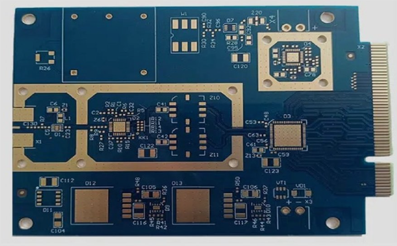
PCB reverse engineering (also called PCB cloning, PCB copying, or PCB design recovery) is the process of analyzing an existing PCB to reconstruct its full design documentation. The goal is to obtain production‑ready files so that the product can be manufactured or upgraded without redesigning the entire circuit.
A complete reverse engineering project typically includes PCB scanning, layer analysis, circuit analysis, PCB layout reconstruction, schematic recovery, Gerber generation, BOM recovery, SMT coordinate extraction, prototyping, and functional verification. Unlike simple copying, reverse engineering recovers the logical design of the whole electronic system.
When Is PCB Reverse Engineering Needed?
- Lost design files: Many legacy products have missing Gerber, layout, or schematic files.
- Obsolete components: ICs from TI, ST, NXP, ADI, Intel, etc., often have 5‑10 year lifecycles; reverse engineering helps find substitutes and optimize designs.
- Industrial equipment maintenance: PLCs, CNC, industrial motherboards, and power devices that are out of production need ongoing support.
- Medical device upgrades: Ultrasound, MRI, CT, and ECG monitors require long‑term maintenance and updates.
- Automotive electronics repair: ECUs, BMS, ADAS modules in electric vehicles often need reverse engineering for repair and upgrades.
2026 PCB Reverse Engineering Price Reference
Costs vary widely by board complexity. The table below shows typical market ranges (USD) for 2026:
| PCB Type | Price Range (USD) | Turnaround |
|---|---|---|
| Single‑layer | 200–500 | 2–4 days |
| Double‑layer | 300–800 | 3–5 days |
| 4‑layer | 800–1,800 | 5–8 days |
| 6–8‑layer | 1,500–3,500 | 7–12 days |
| 10–16‑layer | 3,000–7,000 | 10–20 days |
| HDI PCB | 5,000–12,000 | 2–4 weeks |
| Flex PCB (FPC) | 2,000–6,000 | 2–3 weeks |
| Rigid‑Flex PCB | 4,000–10,000 | 3–5 weeks |
| Rogers RF PCB | 3,000–8,000 | 2–4 weeks |
Prices typically include scanning, layout recovery, schematic recovery, and Gerber generation. Prototyping, SMT, and functional testing are quoted separately.
Cost Breakdown by Complexity
- Basic PCBs ($200–$800): LED lighting, power boards, small appliances, consumer electronics – FR‑4, 1‑2 layers, few components, no BGA. 3‑5 days.
- Medium‑complexity ($1,000–$3,500): Industrial controls, communication, security, medical instruments – 4+ layers, many vias, high‑density components. ~1 week.
- High‑end PCBs ($5,000+): HDI, high‑speed, high‑frequency, automotive, military – require X‑ray, CT scanning, BGA analysis, impedance analysis, multilayer delamination. 2‑4 weeks.
Cost Components
A complete project involves several professional steps, each affecting the final quote:
- Engineering assessment: $100–$300
- Board depopulation: $100–$500
- High‑resolution scanning: $150–$600
- X‑ray inspection: $300–$1,500
- Circuit analysis: $300–$1,500
- Schematic recovery: $500–$2,500
- PCB layout reconstruction: $800–$4,000
- BOM recovery: $200–$800
- Gerber generation: $300–$1,000
- Prototyping: $100–$1,500
- Functional testing: $100–$1,500
Complex projects typically total $2,000–$10,000.
Global Price Comparison
Costs vary by region due to labor, expertise, and manufacturing ecosystem:
- China: Most cost‑effective, with comprehensive one‑stop services. Typical projects $300–$5,000 – saving 30–60% over Western markets.
- Taiwan: Mature technology, moderate cost.
- India: Lower labor costs.
- USA: Higher labor costs, faster delivery – $1,000–$15,000.
- Europe: Strong in industrial automation and medical, but 30–50% higher than Asia.
- Japan: Precision manufacturing leader, but most expensive – complex projects can exceed $20,000.
2022–2026 Price Trends
Demand and prices have been rising steadily:
- 2022: $1,800 (average project)
- 2023: $2,000
- 2024: $2,250
- 2025: $2,500
- 2026: $2,500 (stabilized)
Drivers: increasing complexity (HDI, high‑speed, buried vias), chip obsolescence, and advanced inspection equipment (X‑ray, CT, AOI).
Why Reverse Engineering Is More Cost‑Effective Than Redesign
Redesigning a PCB from scratch typically costs $15,000–$50,000+ and takes months due to architecture, layout, EMC, reliability testing, and certification iterations. Reverse engineering leverages an existing, proven product, allowing rapid recovery of design data and quick transition to prototyping and production – saving 30–70% of R&D costs and reducing lead time from months to weeks. For legacy maintenance, lifecycle extension, or compatibility products, choosing a one‑stop provider like gopcb that combines reverse engineering, PCB fabrication, assembly, and testing further reduces costs and accelerates delivery.
Key Factors Influencing Reverse Engineering Cost
- Layer count: The biggest factor. 1‑2 layers: $200‑800; 4‑layer: $800‑1,800; 6‑8: $1,500‑3,500; 10‑16: $3,000‑7,000; HDI: $5,000‑12,000+. Blind/buried and any‑layer HDI require X‑ray/CT, increasing cost.
- Board size: Larger boards have more data to scan and analyze, raising time and price.
- Material: FR‑4 is standard; Rogers, PTFE, aluminum, ceramic, flex, and rigid‑flex require additional effort for impedance, dielectric, and mechanical properties.
- Component density: High‑density packages (01005, 0201, QFN, BGA, CSP, high‑pin CPUs/FPGAs) need microscopes and precision software, increasing cost.
- Internal structures: Blind vias, buried vias, via‑in‑pad, filled vias, copper coin, embedded components – require X‑ray, CT, and layer‑by‑layer analysis.
- Board condition: Burned, corroded, missing ICs, delaminated, or water‑damaged boards increase difficulty and cost.
- Deliverables: Gerber only is cheaper; full schematics, source files (Altium, Cadence), BOM, SMT coordinates, assembly drawings, test reports, and substitution recommendations add to the cost.
Price Analysis by PCB Type
- Consumer electronics (bluetooth speakers, smart watches, IoT, mice, appliances): $300–$1,500 – simple, few layers.
- Industrial control (PLC, power supplies, servo drives, automation): $1,500–$4,000 – higher reliability and validation.
- Automotive (ECU, BMS, ADAS, infotainment): $2,500–$8,000 – AEC‑Q100, ISO 26262 compliance.
- Medical (ultrasound, ECG, MRI, diagnostic): $3,000–$10,000 – strict quality and traceability.
- High‑frequency/RF (5G, radar, satellite, amplifiers): $3,000–$8,000 – impedance and RF trace recovery.
- HDI (smartphone mainboards, AI modules, high‑speed servers, switches): $5,000–$12,000+ – microvias, buried vias, high density.
PCB Reverse Engineering vs. PCB Cloning
Many confuse the two, but they differ significantly:
- Reverse engineering: Recovers schematics, full layout, editable design files, BOM, supports upgrades – cost $800‑$12,000.
- Cloning (copy): Produces Gerber and possibly BOM but no editable files or schematics – cost $200‑$2,000.
Choose cloning if you only need a production copy; choose reverse engineering if you need to modify, upgrade, or substitute components.
Hidden Costs to Consider
- Prototyping and SMT assembly
- Component procurement (especially obsolete parts)
- Functional testing and firmware validation
- EMC modifications
- Substitute component verification
- International shipping and customs
Using separate vendors for design, fabrication, and assembly increases coordination overhead. A one‑stop provider like gopcb eliminates these extra costs.
How to Reduce PCB Reverse Engineering Costs
- Provide a fully functional board to reduce debugging time.
- Share any existing documentation (partial schematics, BOM, drawings).
- Combine reverse engineering with PCB manufacturing and assembly to avoid duplicate engineering fees.
- Optimize component substitutions during the reverse process to reduce future procurement costs.
- Plan for volume production – apply DFM improvements during recovery to lower manufacturing costs.
Why Choose gopcb for PCB Reverse Engineering?
gopcb is a professional PCB manufacturer with years of experience in both PCB fabrication and PCBA services. We offer a complete one‑stop solution covering reverse engineering, schematic recovery, layout reconstruction, Gerber generation, BOM optimization, component sourcing, quick‑turn prototyping, SMT/DIP assembly, functional testing, pilot runs, and high‑volume production.
Our advanced equipment includes high‑resolution scanning, industrial X‑ray, AOI, precision microscopes, circuit analysis software, and in‑circuit test (ICT) systems – ensuring accuracy for multilayer, HDI, high‑frequency, and rigid‑flex boards.
Typical turnaround: 2‑layer: 3‑5 days; 4‑layer: 5‑8 days; 8‑layer: 7‑12 days; HDI: 2‑4 weeks.
By integrating design recovery, fabrication, assembly, and testing under one roof, we reduce supplier management, cut communication overhead, and accelerate your time‑to‑market.
Explore our services: PCB manufacturing, prototype PCB assembly, turnkey PCB assembly, low‑volume PCB assembly, and high‑volume PCB assembly.
FAQ
1. How much does PCB reverse engineering cost?
Typical projects range from $300 to $12,000, depending on layer count, complexity, packages, and deliverables.
2. How long does it take?
Simple boards: 3‑5 days; multilayer: 1‑2 weeks; complex HDI/RF: 2‑4 weeks.
3. Can multilayer PCBs be reverse‑engineered?
Yes. Professionals use layer stripping, X‑ray, and CT scanning to reconstruct internal traces.
4. Can I get Gerber files from an existing PCB?
Yes. Typically we also provide schematics, layout, drill files, and BOM.
5. Is PCB reverse engineering legal?
It is legal for maintenance, compatibility, authorized product upgrades, and in‑house legacy support. However, third‑party intellectual property must be respected – always obtain necessary permissions.
6. Can a damaged PCB be reverse‑engineered?
Yes, but burned, missing, or severely damaged boards increase difficulty, time, and cost.
7. Can I go directly to production after reverse engineering?
Yes. Once Gerber, BOM, and manufacturing files are complete, we can proceed to prototyping, assembly, and mass production.
Conclusion
As product lifecycles lengthen and documentation becomes lost or obsolete, PCB reverse engineering is increasingly vital for maintaining legacy equipment, upgrading products, and restoring production quickly. Although costs vary widely, reverse engineering typically saves 30–70% of R&D expenses compared to a full redesign and significantly shortens time‑to‑market.
For the best value and fastest turnaround, choose a one‑stop partner with capabilities in reverse engineering, PCB fabrication, PCBA, and testing. gopcb offers proven expertise, advanced equipment, and integrated manufacturing to help you move from board sample to production efficiently – serving industrial controls, automotive, medical, communications, and consumer electronics industries.