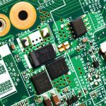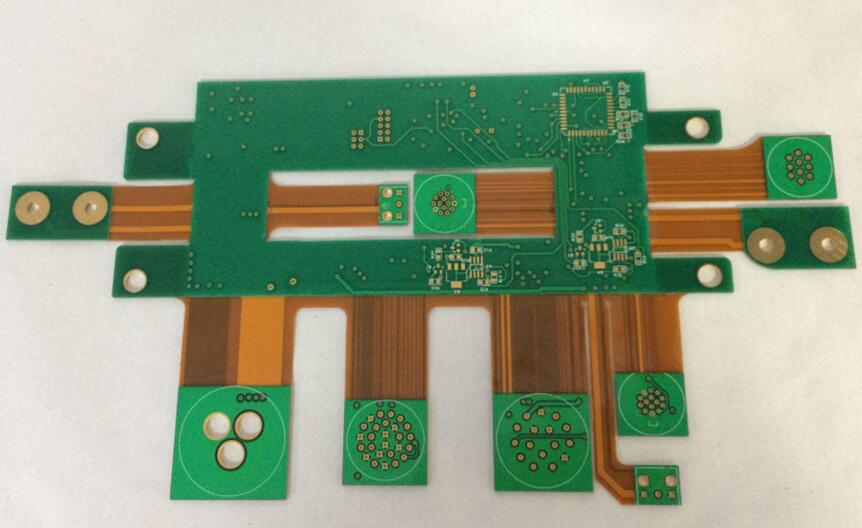
With the rapid development of microelectronic technology, the manufacturing requirements for PCB (Printed Circuit Board) products are continuously increasing. Modern electronic devices are moving toward miniaturization, higher integration, higher performance, and lighter designs. As a result, advanced PCB technologies such as HDI PCB, Rigid-Flex PCB, and high-density multilayer boards have become essential solutions for next-generation electronic applications.
Traditional mechanical drilling methods are becoming increasingly difficult to meet the requirements of high-density interconnection, especially when producing small-diameter holes, deep blind vias, and high aspect ratio structures. Therefore, laser drilling technology has become one of the most important processes in advanced PCB Manufacturing.
Among various laser drilling technologies, CO2 Laser Drilling and UV laser drilling are the two major methods widely used in the PCB industry. Due to its high power output, excellent processing efficiency, and suitability for resin materials, CO₂ laser technology is widely applied in the manufacturing of HDI PCB and Rigid-Flex PCB products.
However, because copper has a high reflection rate for CO₂ laser energy, direct drilling through copper layers remains a major technical challenge. To overcome this limitation, PCB manufacturers have developed various processes, including copper window formation technology, resin-coated copper (RCC) processing, and ultra-thin copper foil solutions.
This article introduces the development background, technical principles, and process advantages of CO2 Laser Drilling technology, explaining how advanced laser processes improve the reliability and manufacturing capability of modern High Precision PCB products.
Development Status of Blind Via Drilling Technology
In addition to traditional mechanical drilling, laser drilling has become a key technology for manufacturing microvias and blind vias in advanced circuit boards.
Currently, CO2 Laser Drilling is widely used in rigid boards and flexible circuit applications because it provides higher drilling efficiency compared with UV laser technology. The main reason is that CO₂ lasers can achieve output power levels of hundreds of watts, providing sufficient energy for high-speed processing.
For conventional rigid and flexible circuit boards, hole diameters are generally larger than those used in semiconductor packaging substrates. Therefore, higher laser energy is required to achieve efficient material removal. In this aspect, CO₂ lasers have significant advantages.
However, copper layers create a major obstacle during laser drilling. Since copper has excellent reflection characteristics against CO₂ laser wavelengths, the laser cannot directly penetrate copper foil efficiently. Therefore, additional processes are required to expose the underlying resin material before laser drilling.
The traditional solution is to create a copper opening window through chemical etching or photolithography processes. After removing the exposed copper area, the CO₂ laser can accurately remove the dielectric resin layer and form a microvia structure.
This process has become an important manufacturing method for HDI PCB production, especially in applications requiring fine line patterns, small vias, and high-density interconnections.
Comparison Between CO₂ Laser Drilling and UV Laser Drilling
UV laser drilling has advantages in processing extremely small holes because of its shorter wavelength and higher precision. However, its relatively low power output limits processing speed and production efficiency.
In contrast, CO2 Laser Drilling provides:
- Higher drilling speed
- Stronger material removal capability
- Better production efficiency
- Lower processing cost for large-scale PCB manufacturing
For applications such as Rigid-Flex PCB, multilayer HDI boards, and high-density interconnection structures, CO₂ laser technology provides an ideal balance between processing efficiency and manufacturing reliability.
However, UV laser drilling still has advantages in applications requiring extremely fine microvias and semiconductor-level precision. Therefore, the selection between CO₂ and UV laser technology depends on PCB structure, material characteristics, hole size requirements, and production volume.
Challenges of Copper Barrier in CO₂ Laser Drilling
The biggest challenge in CO2 Laser Drilling is the interaction between laser energy and copper foil.
Because copper strongly reflects CO₂ laser energy, directly drilling through copper layers may result in:
- Insufficient resin removal
- Irregular via shapes
- Copper damage
- Poor interconnection reliability
To solve this problem, PCB manufacturers generally adopt several methods:
- Copper Window Opening Process
A defined copper window is created above the target drilling position through photolithography and etching processes. The exposed resin area can then be processed using CO₂ laser energy.
- Controlled Copper Thickness Technology
By reducing copper thickness through special processes, laser energy absorption can be improved, allowing more stable microvia formation.
- Ultra-Thin Copper Foil Technology
Ultra-thin copper materials can significantly reduce laser reflection effects and improve drilling accuracy.
Through these advanced technologies, manufacturers can achieve reliable blind via formation while maintaining the electrical performance and mechanical reliability required for modern High Precision PCB products.
Copper Window Opening Technology for CO₂ Laser Drilling
To overcome the copper barrier problem in CO2 Laser Drilling, PCB manufacturers have developed several advanced processing methods. Among them, the copper window opening process is one of the most commonly used technologies for producing Blind Via structures in HDI PCB manufacturing.
1. Copper Window Opening Process
The copper window process begins with the lamination of RCC (Resin Coated Copper) material onto the inner layer circuit. Through photolithography technology, a precisely positioned opening pattern is created on the copper surface.
After exposure and development, the unwanted copper area is removed through an etching process, forming a copper window that exposes the underlying resin layer.
The CO2 Laser Drilling process is then performed through this opening area. The laser energy directly removes the resin material and creates a microvia that connects the outer copper layer with the inner target layer.
However, controlling the accuracy of copper window positioning is a major challenge. Any deviation between the copper opening and the target pad may cause:
- Misalignment of the blind via
- Incomplete electrical connection
- Reduced reliability of the HDI PCB
Therefore, high-precision alignment control is essential during the manufacturing process.
2. Optimization of Copper Window Design
In traditional laser drilling processes, the diameter of the copper window is usually designed to be the same as the final via diameter. However, this method has strict requirements for alignment accuracy.
Due to material expansion and contraction during PCB manufacturing, including:
- Thermal deformation
- Resin shrinkage
- Film expansion during imaging
The actual copper window position may shift slightly, causing the laser drilling position to deviate from the target pad.
To improve process tolerance, modern PCB Manufacturing processes often use a larger copper window design.
For example:
- A microvia with a final diameter of 0.15 mm may use a copper opening diameter of approximately 0.25–0.30 mm.
- The larger opening provides additional process margin and reduces the risk of incomplete drilling.
After the copper window is created, the CO2 Laser Drilling Process can accurately form the microvia according to the inner-layer pad position.
This method improves production yield and is widely used in high-density HDI PCB applications.
Direct Laser Drilling Technology
Another advanced approach is direct laser drilling using ultra-thin copper foil technology.
Instead of creating a large copper window, manufacturers reduce the copper thickness on the surface layer before laser processing. By controlling copper thickness and surface treatment, laser energy absorption can be significantly improved.
During this process:
- A thin copper layer is applied to the PCB surface.
- The copper thickness is reduced through controlled etching.
- Surface oxidation treatment is performed to improve laser absorption.
- The CO2 Laser Drilling system directly forms the microvia structure.
The oxidized copper surface can absorb more laser energy, allowing the laser beam to penetrate the thin copper layer and remove the resin underneath.
This technology provides several advantages:
- Simplified manufacturing process
- Improved drilling accuracy
- Reduced alignment errors
- Higher production efficiency
It is especially suitable for advanced Rigid-Flex PCB and high-density interconnection applications.
Ultra-Thin Copper Foil Technology
Ultra-thin copper foil technology has become an important solution for next-generation High Precision PCB manufacturing.
Traditional copper foil thickness may prevent efficient laser penetration. By reducing copper thickness to approximately several microns, laser processing becomes more stable.
The key requirements for this technology include:
Precise Dielectric Thickness Control
The dielectric layer thickness between copper layers must be carefully controlled. Variations in dielectric thickness can directly affect laser energy distribution and microvia quality.
For reliable Micro Via formation, PCB manufacturers must maintain:
- Stable resin thickness
- Uniform material characteristics
- Accurate laser energy control
Clean Via Bottom Processing
After laser drilling, the bottom of the microvia must be completely clean.
Any remaining resin residue or contamination may negatively affect:
- Copper plating quality
- Electrical conductivity
- Long-term reliability
Therefore, advanced cleaning and desmear processes are required before the subsequent copper plating process.
Process Control Requirements for Reliable Laser Drilling
The quality of CO2 Laser Drilling depends not only on laser equipment performance but also on complete process control.
Important control factors include:
1. Material Selection
High-quality RCC materials and dielectric materials must provide stable thickness and excellent laser processing characteristics.
2. Laser Parameter Optimization
Laser power, pulse frequency, drilling speed, and energy distribution must be precisely adjusted according to:
- PCB material
- Copper thickness
- Via diameter
- Layer structure
3. Process Monitoring
Advanced inspection methods are required to verify:
- Via diameter accuracy
- Hole wall quality
- Copper plating reliability
- Interlayer connection performance
Through strict process management, manufacturers can achieve high-quality Blind Via structures for advanced electronic products.

Kingda Advanced PCB Manufacturing Capability
With the continuous development of electronic products toward miniaturization and high integration, the demand for advanced HDI PCB, Rigid-Flex PCB, and High Precision PCB continues to grow.
Kingda focuses on providing reliable PCB Manufacturing solutions, including advanced multilayer PCB fabrication, high-density interconnection technology, laser drilling processes, and precision manufacturing control.
By applying advanced equipment, strict quality management, and optimized production processes, Kingda supports customers in developing high-performance electronic products requiring excellent signal integrity, reliability, and miniaturized designs.
Conclusion
The development of CO2 Laser Drilling technology has significantly improved the manufacturing capability of modern HDI PCB and Rigid-Flex PCB products.
Although copper reflection remains a challenge, technologies such as copper window opening, ultra-thin copper foil processing, and optimized laser parameters have successfully improved microvia formation reliability.
As electronic devices continue to demand smaller sizes, higher performance, and greater integration, advanced Laser Drilling Process technology will remain a key foundation for future PCB Manufacturing development.
Through continuous process innovation and precision manufacturing capability, Kingda is committed to providing high-quality PCB solutions that meet the evolving requirements of the global electronics industry.