Essential PCB Design Basics Every Engineer Should Know
A reliable printed circuit board starts with a well-planned design. From schematic verification and component placement to layer stack-up, power distribution, grounding, routing, and manufacturability, every design decision can influence the electrical performance, reliability, and production cost of the final board.
Whether you are developing a prototype or preparing for volume production, understanding the fundamentals of PCB Design can help prevent costly redesigns and manufacturing problems.
This guide explains several essential principles that engineers should consider when developing a reliable PCB.
1. Verify FPGA Pin Assignments Before PCB Design
If the circuit includes an FPGA, pin assignments should be verified before completing the schematic and PCB layout.
Some FPGA pins have dedicated functions, such as configuration, clocking, power, reference voltage, or high-speed interfaces. These pins may not be interchangeable with ordinary I/O pins.
Before starting the PCB layout, engineers should therefore verify:
- FPGA pin functions
- Power and ground requirements
- Configuration pins
- Clock inputs and outputs
- High-speed interfaces
- I/O voltage compatibility
- Differential-pair assignments
- Bank voltage requirements
Using the FPGA vendor’s development software to validate pin assignments can prevent major layout problems later in the design process.
For complex projects, professional PCB Design services can also help evaluate component placement, stack-up, high-speed routing, and manufacturability before fabrication.
2. Plan the PCB Layer Stack-Up Carefully
The layer stack-up is one of the most important decisions in multilayer board design.
A four-layer PCB may use a structure such as:
- Layer 1: Signal and component layer
- Layer 2: Ground plane
- Layer 3: Power plane or signal layer
- Layer 4: Signal and component layer
A six-layer PCB can provide additional flexibility for separating high-speed signals, power, and ground. One possible structure is:
- Layer 1: Signal / Components
- Layer 2: Ground
- Layer 3: High-speed signals
- Layer 4: Power
- Layer 5: Ground
- Layer 6: Signal / Components
However, there is no universal stack-up that is suitable for every design. The optimal structure depends on signal speed, impedance requirements, routing density, power distribution, material properties, thermal requirements, and manufacturing capability.
For advanced Multilayer PCB projects, engineers should define the stack-up early instead of treating it as a manufacturing-stage decision.
3. Use Power Planes and Copper Areas Appropriately
Modern electronic systems often contain several power rails. For example, an FPGA and DSP system may use 5 V, 3.3 V, 1.8 V, and 1.2 V supplies.
Different power rails should be handled according to their current requirements, distribution area, noise sensitivity, and electrical function.
Main Power Rails
A widely distributed rail such as 3.3 V may benefit from a dedicated plane or large copper area when the stack-up and design requirements allow it.
An input rail such as 5 V may only need to supply a specific section of the board. In this case, appropriately sized copper traces or copper areas may be sufficient.
Core Power Rails
Low-voltage FPGA or processor core supplies such as 1.2 V and 1.8 V often require careful placement and routing because they may supply high-current loads over relatively short paths.
Instead of routing these power connections across the entire PCB with long narrow traces, engineers can often improve the design by placing related components close together and using appropriately sized copper areas.
The objective is to minimize:
- Voltage drop
- Power distribution impedance
- Current-loop area
- Unnecessary routing distance
- Thermal concentration
The final power-distribution strategy should always be based on current requirements and the specific PCB stack-up rather than applying a single rule to every design.
4. Keep Adjacent Signal Layers Properly Referenced
Signal routing on different layers should be planned together with their reference planes.
Instead of simply routing adjacent layers in arbitrary directions, engineers should consider electromagnetic coupling, return-current paths, layer-to-layer capacitance, and routing density.
For multilayer high-speed designs, maintaining a continuous reference plane beneath critical signals is often more important than simply changing routing direction.
A well-designed stack-up can help control:
- Crosstalk
- Electromagnetic interference
- Return-path discontinuities
- Signal reflections
- Controlled impedance
- Power integrity
This is particularly important when designing high-speed digital interfaces, RF circuits, networking hardware, and communication equipment.
5. Separate Analog and Digital Circuits Carefully
Mixed-signal PCB designs require careful management of analog and digital circuitry.
A common design approach is to separate sensitive analog circuitry from noisy digital circuitry during component placement.
For example:
- Analog components should be grouped within a dedicated functional area.
- Digital switching circuits should be kept away from sensitive analog nodes.
- High-current switching paths should not cross sensitive analog signal paths.
- ADC and DAC interfaces should receive special attention.
- Ground-return paths should be carefully evaluated.
However, analog and digital grounds should not automatically be split into isolated islands in every design.
The correct grounding strategy depends on the converter architecture, current-return paths, signal frequencies, power distribution, and system-level EMC requirements.
In many mixed-signal systems, maintaining a continuous reference plane and controlling return-current paths is preferable to creating unnecessary ground splits.
For challenging designs, Signal Integrity and EMC considerations should be incorporated during the initial layout rather than being addressed after fabrication.
6. Treat PCB Design as an Iterative Engineering Process
PCB design should not be considered a simple process of drawing traces.
A reliable workflow involves continuous verification and feedback between the schematic, layout, mechanical structure, electrical requirements, and manufacturing constraints.
A typical workflow may include:
Step 1: Schematic Review
Check:
- Power connections
- Ground connections
- Component values
- Net names
- Signal direction
- Interface compatibility
- Unused pins
- Critical components
Power and ground connections deserve particular attention because mistakes in these networks can affect the entire system.
Step 2: PCB Footprint Verification
Every PCB footprint should be verified against the component manufacturer’s mechanical dimensions.
Check:
- Pad dimensions
- Pin numbering
- Component outline
- Courtyard
- Pin pitch
- Thermal pads
- Polarity markings
- Height restrictions
Incorrect footprints can cause assembly failures even when the schematic itself is electrically correct.
Step 3: Component Placement
Component placement should consider:
- Functional blocks
- Signal-flow direction
- Power distribution
- Thermal management
- Mechanical constraints
- Connector locations
- High-speed signal paths
- Assembly requirements
Step 4: Routing and Verification
During routing, engineers should continuously check critical nets, power distribution, return paths, spacing, differential pairs, impedance requirements, and design rules.
Step 5: DFM Review
Before manufacturing, the completed layout should undergo Design for Manufacturability analysis.
A professional PCB Manufacturing partner can review issues such as:
- Minimum trace width
- Minimum spacing
- Drill diameter
- Annular ring
- Copper thickness
- Via structures
- Solder mask clearance
- Board outline
- Layer registration
- Impedance requirements
- Manufacturing tolerances
Early DFM analysis can reduce redesigns, production delays, and manufacturing costs.
7. Place Crystal Oscillators Close to Their ICs
Crystal oscillators and clock sources should generally be placed close to the IC they serve.
Long clock traces can increase the possibility of:
- Noise coupling
- Signal distortion
- Unwanted radiation
- Timing problems
- Electromagnetic interference
The crystal network should also follow the semiconductor manufacturer’s recommended layout guidelines.
Avoid placing unrelated high-speed traces directly beneath or too close to sensitive oscillator structures when the reference design recommends a clear area.
For systems with multiple clock consumers, the clock distribution strategy should be designed according to the required topology, timing budget, impedance, and signal integrity requirements.
8. Connector Pin Assignment Can Simplify PCB Routing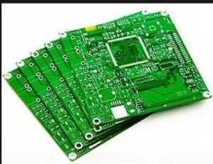
Connector pin assignments have a major influence on PCB routing difficulty.
When designing a connector interface, engineers should consider the physical arrangement of the mating connector, signal direction, differential pairs, power pins, ground pins, and return paths.
For board-to-board connections, pin assignments can sometimes be optimized so that signals naturally cross or align according to the physical orientation of the two boards.
However, connector pin assignment should be determined by the actual mechanical and electrical requirements rather than relying on a fixed numbering rule.
For high-speed interfaces, it is especially important to maintain:
- Differential-pair integrity
- Reference-plane continuity
- Controlled impedance
- Appropriate ground spacing
- Short signal paths
- Low-inductance return paths
9. Optimize Module-to-Module Signal Connections
When two functional modules communicate with each other, the PCB designer should consider the physical orientation of the modules before finalizing pin assignments.
If two modules are located on the same side of a PCB, mirrored signal arrangements may sometimes simplify routing.
If the modules are located on opposite sides, a different pin arrangement may reduce crossing and via transitions.
The objective is not to follow one universal pin-numbering rule, but to optimize the physical signal path.
A good PCB Layout should minimize unnecessary routing complexity while maintaining electrical performance and manufacturability.
10. Minimize Power and Ground Loop Areas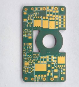
Power and ground routing should be considered as a complete current loop rather than as two independent connections.
A large loop area can increase susceptibility to electromagnetic interference and increase unwanted radiation.
A smaller loop provides a shorter return path and can reduce loop inductance.
Therefore, engineers should try to keep power and return paths physically close when practical.
This is particularly important for:
- High-speed switching circuits
- DC/DC converters
- Motor-control circuits
- RF circuits
- High-current power supplies
- Fast digital interfaces
At the same time, signal traces should not be routed excessively close and parallel for long distances when doing so increases crosstalk.
11. Select PCB Materials According to Application Requirements
Material selection should be considered early in the design process.
Standard FR-4 is suitable for a large range of general-purpose electronic products. Higher-Tg materials may be appropriate for applications with higher thermal requirements, while low-loss high-frequency materials may be required for RF and high-speed applications.
Important material parameters include:
- Glass transition temperature (Tg)
- Decomposition temperature (Td)
- Coefficient of thermal expansion (CTE)
- Dielectric constant (Dk)
- Dissipation factor (Df)
- Thermal conductivity
- Copper compatibility
- Mechanical stability
For high-frequency designs, dielectric properties and loss characteristics can directly influence impedance and insertion loss.
PCB Capabilities & Materials
12. Consider EMI and Signal Integrity During the Initial Design
EMI problems are often much easier to prevent during PCB layout than to correct after fabrication.
Important design factors include:
- Continuous reference planes
- Short return-current paths
- Appropriate layer stack-up
- Controlled impedance
- Differential-pair routing
- Power integrity
- Grounding strategy
- Decoupling capacitor placement
- Switching-current loop minimization
- High-speed interface routing
For high-speed circuits, trace geometry and dielectric thickness should be designed together with the selected PCB material and stack-up.
A professional Signal Integrity approach can help evaluate reflection, crosstalk, impedance discontinuities, and transmission-line behavior before prototype fabrication.
13. Use DFM Before Releasing Production Files
One of the most effective ways to reduce PCB production problems is to perform DFM analysis before manufacturing.
Typical DFM checks include:
Trace and Spacing
Verify that trace widths and clearances are compatible with the manufacturer’s process capability.
Via and Drill Design
Check drill diameter, aspect ratio, hole-to-hole spacing, hole-to-copper clearance, and annular ring requirements.
Copper Distribution
Large differences in copper density can affect etching, plating, lamination, and board flatness.
Solder Mask and Silkscreen
Ensure that solder-mask openings and silkscreen markings do not interfere with pads, vias, or component assembly.
Stack-Up and Impedance
For controlled-impedance designs, confirm that the proposed stack-up, dielectric thickness, copper thickness, and material properties are consistent with the target impedance.
A manufacturer with integrated engineering and fabrication capabilities can identify these problems before production begins.
PCB Manufacturing Capabilities
14. Verify the Finished PCB Through Inspection and Testing
PCB quality cannot be evaluated by visual inspection alone.
Depending on the application and production volume, inspection and testing may include:
- Automated Optical Inspection (AOI)
- X-ray inspection
- Flying probe testing
- Electrical testing
- In-circuit testing
- Functional testing
- Dimensional inspection
- Cross-section analysis
- Impedance testing
For assembled PCBs, additional inspection may include solder paste inspection, AOI, X-ray inspection, and functional verification.
Testing requirements should be defined according to the board’s intended application, reliability requirements, and production stage.
15. Design for Both Electrical Performance and Manufacturing
A PCB that works correctly in simulation is not necessarily a PCB that can be manufactured efficiently.
Successful PCB development requires coordination between:
- Circuit design
- Component selection
- PCB layout
- Layer stack-up
- Signal integrity
- Power integrity
- Thermal management
- Mechanical design
- DFM
- Assembly
- Testing
This is why PCB Manufacturing requirements should be considered from the beginning of the design process.
A design with extremely narrow traces, unnecessarily complex vias, excessive tolerances, or difficult component placement may increase manufacturing cost without providing meaningful electrical benefits.
The best PCB design is therefore a balance between electrical performance, mechanical requirements, manufacturing capability, reliability, and total cost.
What to Confirm Before Production
The notes below group the main process checks into a quick reference.
1. Verify FPGA Pin Assignments Before PCB Design: review the production data and close any deviation before the next build.
2. Plan the PCB Layer Stack-Up Carefully: confirm the requirements, process settings and inspection records at first-article approval.
3. Use Power Planes and Copper Areas Appropriately: record the agreed limits and verify them again in the production lot.
4. Keep Adjacent Signal Layers Properly Referenced: check the drawing, process sheet and inspection plan before release.
5. Separate Analog and Digital Circuits Carefully: treat this as a repeat-order checkpoint and keep the result with the lot record.
6. Treat PCB Design as an Iterative Engineering Process: review the production data and close any deviation before the next build.
7. Place Crystal Oscillators Close to Their ICs: confirm the requirements, process settings and inspection records at first-article approval.
8. Connector Pin Assignment Can Simplify PCB Routing: record the agreed limits and verify them again in the production lot.
Conclusion
Reliable PCB development begins long before the circuit board reaches the factory.
Engineers should verify schematic and FPGA pin assignments, establish an appropriate layer stack-up, optimize power and ground distribution, control signal return paths, separate sensitive functional areas, place clock components carefully, and evaluate EMI and signal integrity during the layout process.
For complex boards, DFM should be integrated into the engineering workflow before production data is released.
By combining robust PCB Design, optimized PCB Layout, appropriate materials, controlled Multilayer PCB construction, and reliable PCB Manufacturing, engineers can reduce design errors, improve production yield, control development costs, and achieve more reliable electronic products.