30-Layer PCB Manufacturer for High-Performance Electronics
As electronic systems continue to become smaller, faster, and more complex, conventional circuit board structures are often unable to provide sufficient routing capacity and electrical performance. A 30-layer PCB offers a high-density platform for integrating signal, power, and ground networks within a compact board structure.
These high-layer-count circuit boards are commonly considered for demanding applications such as 5G communication equipment, AI servers, high-performance computing systems, aerospace electronics, advanced medical equipment, industrial control systems, and other high-density electronic products.
Choosing the right 30-layer PCB manufacturer is therefore critical. High-layer-count PCB production requires precise stack-up engineering, controlled lamination, accurate layer registration, advanced drilling, reliable copper plating, impedance control, and comprehensive inspection.
GOPCBA provides advanced PCB fabrication and manufacturing services covering multilayer, HDI, high-speed, high-frequency, high-TG, rigid-flex, heavy-copper, and controlled-impedance PCB technologies.
Why 30-Layer PCB Manufacturing Is Technically Challenging
Compared with conventional two-layer or standard multilayer boards, a 30-layer design introduces substantially greater manufacturing complexity. As the number of conductive and dielectric layers increases, small process variations can accumulate and affect electrical, mechanical, and structural performance.
A reliable multilayer PCB manufacturing process must carefully control several critical factors, including:
- Layer stack-up and dielectric thickness
- Inner-layer registration
- Lamination temperature and pressure
- Copper thickness
- Drilling accuracy
- Via reliability
- Impedance consistency
- Board thickness and warpage
- Thermal expansion
- Surface finish
- Electrical testing
For high-layer-count boards, manufacturability should be considered during the design stage rather than after the PCB layout has been completed.
Advanced Stack-Up Engineering for 30-Layer PCBs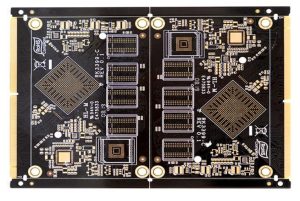
The stack-up is one of the most important factors in high-layer-count PCB manufacturing. A 30-layer board may contain multiple signal layers, power planes, ground planes, and specialized layers for high-speed or high-frequency circuits.
The layer arrangement should be designed according to the electrical and mechanical requirements of the application.
For high-speed systems, signal layers should generally be positioned close to stable reference planes. This helps establish predictable return-current paths and supports controlled impedance.
Power and ground layers can also be strategically distributed throughout the stack-up to improve power integrity, reduce electromagnetic interference, and provide more stable electrical performance.
A properly balanced stack-up can also reduce mechanical stress during lamination and minimize the risk of board warpage.
Before production, engineers should verify:
- Total layer count
- Finished board thickness
- Copper thickness
- Dielectric materials
- Resin content
- Signal-layer arrangement
- Power and ground plane distribution
- Controlled-impedance requirements
- Minimum trace and spacing
- Via structures
- Surface finish
- Manufacturing tolerances
For complex multilayer designs, early engineering review can significantly reduce manufacturing risks.
Precision Lamination for High-Layer-Count PCB Manufacturing
Lamination is one of the most critical processes in 30-layer PCB fabrication.
The inner-layer circuits, cores, prepreg materials, and copper foils must be combined into a stable multilayer structure under carefully controlled temperature and pressure conditions.
Poor lamination control can result in:
- Layer misalignment
- Internal voids
- Delamination
- Resin starvation
- Excessive board thickness variation
- Warpage
- Dielectric inconsistency
- Reduced long-term reliability
As the layer count increases, registration becomes increasingly important. Even relatively small dimensional changes during heating and cooling can affect the final alignment between different layers.
For this reason, advanced PCB manufacturing requires controlled lamination processes, appropriate material selection, accurate stack-up calculations, and consistent process monitoring.
Fine-Line Routing and High-Density Interconnection
A 30-layer board is often selected because the electronic system requires substantially more routing capacity than a conventional PCB can provide.
Increasing layer count provides additional routing space, but high-density designs may also require fine-line technology and advanced via structures.
This is where HDI PCB technology can provide additional design flexibility.
HDI structures can incorporate microvias, blind vias, buried vias, stacked microvias, and sequential buildup structures. These technologies allow electrical connections to be created between selected layers while reducing the space consumed by conventional through-hole vias.
For compact electronic systems, HDI technology can provide:
- Higher routing density
- Smaller component breakout areas
- Shorter electrical connections
- Improved BGA routing
- Better utilization of PCB space
- Greater flexibility for complex layouts
However, HDI manufacturing requires tighter control of laser drilling, copper plating, via filling, lamination, and layer registration. The selected structure should therefore be compatible with the PCB manufacturer’s actual manufacturing capabilities.
High-Speed Signal Integrity in 30-Layer PCBs
High-layer-count PCBs are increasingly used in systems that process large amounts of high-speed data. AI servers, networking equipment, telecommunications hardware, computing platforms, and advanced industrial electronics may require controlled impedance and carefully engineered signal paths.
A high-speed PCB must maintain stable electrical characteristics throughout the signal transmission path.
Important design and manufacturing considerations include:
- Controlled impedance
- Stable dielectric thickness
- Appropriate reference planes
- Low-loss materials
- Accurate copper geometry
- Short return-current paths
- Reduced crosstalk
- Reduced signal reflection
- Consistent layer registration
The stack-up directly affects impedance because trace width, copper thickness, dielectric thickness, and dielectric constant all influence the electrical characteristics of the transmission line.
For this reason, impedance requirements should be considered during stack-up development rather than treated as a final inspection item.
Materials for 30-Layer PCB Manufacturing
Material selection becomes increasingly important as PCB layer count, operating frequency, data rate, and thermal requirements increase.
Standard FR-4 materials may be suitable for many applications, while high-TG, low-loss, or high-frequency materials may be required for more demanding designs.
Material selection may depend on:
- Operating temperature
- Signal frequency
- Data rate
- Dielectric constant
- Dissipation factor
- Thermal expansion
- Mechanical stability
- Required reliability
- Cost targets
For high-speed and high-frequency applications, lower-loss materials can help reduce signal attenuation. For high-temperature applications, high-TG materials can provide improved thermal stability.
The material system should also be compatible with the selected lamination process and the complete PCB stack-up.
Precision Drilling, Plating, and Via Reliability
Drilling is another important manufacturing process for a 30-layer circuit board.
A high-layer-count PCB may contain conventional through-holes as well as blind, buried, and microvia structures. Each via type has different manufacturing requirements.
Mechanical drilling is commonly used for conventional through-holes, while laser drilling can be used for microvias and certain HDI structures.
After drilling, copper plating establishes electrical connections between conductive layers. Plating quality must be carefully controlled because insufficient or inconsistent copper deposition can affect electrical conductivity and long-term mechanical reliability.
Important process controls include:
- Hole diameter
- Hole position
- Hole-wall quality
- Copper plating thickness
- Aspect ratio
- Via filling requirements
- Surface treatment
- Electrical continuity
For advanced PCB structures, cross-sectional analysis and other inspection methods can be used to verify internal construction.
Quality Control for 30-Layer PCB Production
The complexity of a 30-layer PCB makes comprehensive quality control essential.
Quality assurance should begin with incoming materials and continue through inner-layer fabrication, lamination, drilling, plating, surface finishing, electrical testing, and final inspection.
Typical inspection technologies may include:
Automated Optical Inspection
AOI systems can inspect inner and outer circuit patterns for defects such as opens, shorts, missing copper, unwanted copper, and dimensional abnormalities.
X-Ray Inspection
X-Ray inspection can provide information about internal structures that cannot be visually inspected from the PCB surface. It can be particularly useful for advanced multilayer and HDI structures.
Cross-Section Analysis
Microsection analysis can be used to examine layer registration, copper thickness, hole-wall plating, via structures, and internal construction.
Electrical Testing
Electrical testing verifies circuit continuity and isolation to help identify manufacturing defects before shipment.
Process Traceability
Manufacturing records should connect raw materials, process parameters, inspection results, and finished products. Traceability helps manufacturers investigate quality issues and maintain consistent production performance.
Applications of 30-Layer PCBs
The high routing density and structural flexibility of a 30-layer circuit board make it suitable for demanding electronic systems.
AI Servers and High-Performance Computing
AI and HPC platforms require high-speed interconnections, high-density power distribution, and stable signal transmission. A 30-layer structure can provide additional space for signal, power, and ground networks.
5G and Telecommunications
Telecommunications equipment can require high-speed digital interfaces, RF circuits, multiple power domains, and controlled-impedance transmission paths.
Aerospace and Satellite Electronics
Aerospace systems may require compact, highly reliable electronics capable of operating under demanding environmental conditions. High-layer-count PCB structures can support complex system integration within limited physical space.
Medical Electronics
Advanced medical equipment can require high-density electronics, reliable signal transmission, and long-term operational stability. A carefully engineered multilayer structure can help integrate complex electronic functions.
Industrial Control Systems
Industrial equipment often combines control circuits, communication interfaces, power management, and sensor systems. A high-layer-count PCB can provide sufficient routing capacity while maintaining functional separation between different circuit domains.
Automotive Electronics
Modern automotive systems increasingly integrate ADAS, vehicle networking, battery management, power electronics, infotainment, and control functions. Depending on the application, multilayer and HDI structures can provide the required density and electrical performance.
30-Layer PCB Manufacturing From Prototype to Production
Selecting a manufacturing partner that can support both prototype development and production manufacturing can simplify the transition from engineering validation to volume production.
A professional PCB manufacturing workflow can include:
- Gerber and design file review
- DFM analysis
- Stack-up verification
- Material selection
- Inner-layer circuit fabrication
- Multilayer lamination
- Mechanical and laser drilling
- Copper plating
- Circuit formation
- Solder mask application
- Surface finishing
- Electrical testing
- Final inspection
- Packaging and shipment
Engineering review at the beginning of the project can identify potential problems with layer registration, material availability, impedance, drilling, copper distribution, and manufacturability before production begins.
Choosing a Reliable 30-Layer PCB Manufacturer
Not every PCB factory is equipped to manufacture high-layer-count circuit boards. When evaluating a 30-layer PCB manufacturer, buyers should consider both technical capability and production consistency.
Important evaluation criteria include:
- High-layer-count manufacturing capability
- Multilayer lamination experience
- HDI and microvia capability
- Controlled-impedance manufacturing
- High-speed PCB experience
- High-frequency material compatibility
- Precision drilling and plating
- Advanced inspection equipment
- Engineering and DFM support
- Prototype and production capability
- Quality traceability
- Consistent manufacturing processes
GOPCBA provides PCB fabrication and assembly solutions for complex electronic products, supporting multilayer, HDI, high-speed, high-frequency, rigid-flex, heavy-copper, high-TG, and controlled-impedance PCB requirements.
For projects requiring additional manufacturing support, customers can also combine PCB fabrication with PCB assembly, component sourcing, SMT, THT, inspection, and testing through an integrated manufacturing workflow.
Design and Quality Review
This summary highlights the points that most often affect yield.
- Why 30-Layer PCB Manufacturing Is Technically Challenging: review the production data and close any deviation before the next build.
- Advanced Stack-Up Engineering for 30-Layer PCBs: confirm the requirements, process settings and inspection records at first-article approval.
- Precision Lamination for High-Layer-Count PCB Manufacturing: record the agreed limits and verify them again in the production lot.
- Fine-Line Routing and High-Density Interconnection: check the drawing, process sheet and inspection plan before release.
- High-Speed Signal Integrity in 30-Layer PCBs: treat this as a repeat-order checkpoint and keep the result with the lot record.
- Materials for 30-Layer PCB Manufacturing: review the production data and close any deviation before the next build.
- Precision Drilling, Plating, and Via Reliability: confirm the requirements, process settings and inspection records at first-article approval.
- Quality Control for 30-Layer PCB Production: record the agreed limits and verify them again in the production lot.
Conclusion
A 30-layer circuit board represents a significant step beyond conventional multilayer PCB manufacturing. Its successful production requires coordinated control of stack-up design, materials, lamination, layer registration, drilling, copper plating, impedance, signal integrity, and quality inspection.
For applications such as AI computing, telecommunications, aerospace, medical electronics, industrial control, and advanced automotive systems, high-layer-count PCB technology can provide the routing density and electrical architecture needed for increasingly complex products.
The key to reliable production is not simply increasing the number of layers. It is combining appropriate materials, optimized stack-up engineering, advanced manufacturing processes, rigorous inspection, and experienced engineering support.
GOPCBA supports advanced PCB manufacturing from prototype development through production, helping customers develop reliable high-layer-count circuit boards for demanding electronic applications.