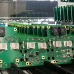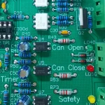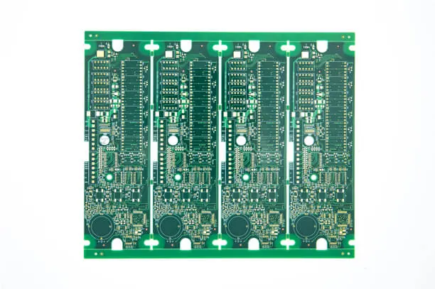
Custom BMS PCB Manufacturing for New Energy Vehicles
A BMS PCB is a critical hardware platform for battery management systems in electric and new energy vehicles. It supports battery voltage and temperature monitoring, cell balancing, power management, communication, and protection functions. Unlike general-purpose circuit boards, automotive BMS boards must operate reliably under temperature fluctuations, vibration, humidity, electrical noise, and long service cycles.
For this reason, Automotive PCB Manufacturing requires careful control of material selection, circuit fabrication, multilayer construction, surface finishing, dimensional accuracy, and electrical testing. A well-engineered BMS circuit board must not only satisfy the electrical requirements of the battery management system but also maintain stable mechanical and electrical performance throughout the vehicle’s operating life.
GOPCBA provides advanced PCB Manufacturing Services for automotive electronics, including multilayer, HDI, high-frequency, high-TG, heavy-copper, rigid-flex, and controlled-impedance PCB technologies. These capabilities allow BMS projects to be manufactured according to their specific electrical, thermal, mechanical, and reliability requirements.
1. Substrate Selection and Material Preparation

The manufacturing process for a BMS PCB begins with selecting an appropriate substrate. The material must be compatible with the electrical and environmental conditions of the battery management system.
During material selection, engineers typically consider:
- Operating temperature range
- Dielectric strength
- Thermal stability
- Mechanical strength
- Copper thickness
- Dimensional stability
- Layer count
- Power requirements
- Space limitations
For automotive applications, high-TG materials can be considered when greater thermal stability is required. For power-related BMS circuits, copper thickness and thermal management also need to be evaluated according to the expected current load.
For complex battery management systems, a Multilayer PCB can provide additional routing space and allow power, ground, sensing, communication, and control circuits to be distributed across different layers.
Material preparation is equally important. Before subsequent processing, PCB materials must be properly cleaned and conditioned to remove contaminants and ensure stable adhesion between copper and dielectric layers.
Surface preparation can include cleaning and micro-etching processes. Proper control of these parameters helps reduce the risk of poor copper adhesion, delamination, and other manufacturing defects.
2. Circuit Pattern Transfer and PCB Fabrication
Precise circuit pattern transfer is one of the most important stages in Automotive PCB Manufacturing.
The circuit pattern is transferred onto the copper surface according to the customer’s PCB design data. High-precision exposure and developing processes are used to reproduce the required trace width, spacing, pads, and other circuit features.
For BMS applications, manufacturing accuracy is especially important because the board may contain:
- Battery voltage sensing circuits
- Temperature sensing circuits
- Cell balancing circuits
- Communication interfaces
- Power distribution networks
- Protection circuits
- Microcontroller connections
After pattern transfer, unwanted copper is removed through etching to form the required circuit pattern. Etching parameters must be carefully controlled to minimize undercutting, over-etching, burrs, and dimensional deviations.
For high-density designs, an HDI PCB structure can provide greater routing density within a limited board area. Microvias, blind vias, buried vias, and fine-line technology can help engineers optimize electrical connections while reducing board size.
3. Multilayer Construction and Lamination
Many modern battery management systems require more complex circuit architectures. A Multilayer PCB can separate power, ground, sensing, control, and communication functions across different layers.
The multilayer manufacturing process normally involves combining inner-layer circuits, cores, and prepreg materials through controlled lamination.
Important lamination parameters include:
- Temperature
- Pressure
- Heating rate
- Cooling rate
- Resin flow
- Layer registration
- Dielectric thickness
Poor lamination control can result in layer misalignment, internal voids, delamination, resin starvation, or board warpage.
For automotive BMS applications, dimensional stability is particularly important because variations in the multilayer structure can influence drilling accuracy, impedance, electrical spacing, and final assembly performance.
For advanced automotive circuit designs, GOPCBA also provides Automotive Multilayer PCB Manufacturing solutions covering high-density interconnection, thermal management, controlled impedance, multilayer construction, and automotive electronics.
4. Surface Finishing for Reliability and Assembly
Surface finishing is another important part of BMS PCB production. The selected finish must be compatible with the assembly process, connector requirements, electrical performance, and expected service environment.
Common surface finishes include:
- ENIG
- ENEPIG
- Immersion tin
- Immersion silver
- OSP
ENIG provides a flat surface, good oxidation resistance, and reliable solderability, making it suitable for many high-density electronic assemblies.
Immersion tin can provide good solderability and may offer a cost-effective solution for certain applications.
OSP forms an organic protective layer over exposed copper and can provide good solderability while maintaining a relatively simple surface structure.
The correct surface finish depends on the specific BMS design, component package, assembly process, environmental requirements, and expected product life.
For high-density and fine-pitch BMS assemblies, surface flatness and finish consistency are particularly important because they can affect component placement and soldering quality.
5. Precision Routing, Drilling, and Edge Processing
The physical dimensions of a BMS circuit board must match the battery pack and electronic module installation space.
During custom production, PCB manufacturers may use CNC routing, mechanical drilling, laser drilling, or other precision processes depending on the board structure.
Critical dimensions may include:
- Overall board dimensions
- Mounting holes
- Positioning holes
- Slots
- Connector openings
- Component clearance areas
- Edge profiles
For an HDI PCB, laser-drilled microvias can be used to create compact interconnection structures. Blind and buried vias can also help reduce routing congestion and improve space utilization.
After machining, PCB edges and openings should be inspected and processed to remove burrs or unwanted residues. Accurate edge processing helps ensure proper mechanical installation and reduces the risk of interference with surrounding components.
For flexible or rigid-flex BMS applications, the mechanical structure must also account for bending requirements and stress concentration.
6. Electrical Performance and Signal Integrity
BMS boards often combine low-level sensing signals with power and communication circuits. This makes electrical design and manufacturing consistency essential.
For advanced designs, PCB layout and manufacturing should consider:
- Trace width and spacing
- Copper thickness
- Ground planes
- Power distribution
- Return paths
- Dielectric thickness
- Signal isolation
- Impedance control
- Electromagnetic interference
GOPCBA provides PCB Design & Layout Services covering multilayer PCB design, HDI structures, high-speed circuits, high-frequency applications, impedance control, blind and buried vias, and manufacturability analysis.
For BMS designs containing high-speed communication interfaces, controlled-impedance structures may be required to maintain stable signal transmission.
A manufacturing process that maintains consistent dielectric thickness, copper geometry, layer registration, and stack-up configuration can help improve electrical consistency from prototype through production.
7. Inspection and Quality Control
Quality control is essential throughout PCB Manufacturing Services, particularly for automotive applications where long-term reliability is critical.
Depending on the project requirements, inspection may include:
- Automated optical inspection (AOI)
- Electrical testing
- Flying probe testing
- Dimensional inspection
- Impedance testing
- X-ray inspection
- Cross-section analysis
- Surface finish inspection
- Visual inspection
Electrical testing helps identify open circuits, short circuits, and other connectivity problems.
AOI can detect circuit-pattern defects such as missing copper, excessive copper, spacing problems, and other visible manufacturing abnormalities.
For complex multilayer or HDI structures, X-ray inspection and cross-sectional analysis can provide additional information about internal structures, vias, and layer alignment.
Automotive projects can also benefit from production traceability. Material information, process parameters, inspection records, and production batch information can be maintained to support quality analysis and process improvement.
8. BMS PCB Applications in New Energy Vehicles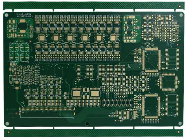
A custom BMS PCB can be used across different battery management architectures and vehicle platforms.
Typical applications include:
Battery Monitoring Systems
The PCB provides electrical connections for monitoring battery cell voltage, temperature, current, and other operating parameters.
Cell Balancing Systems
BMS circuits can support active or passive balancing functions to help maintain appropriate voltage relationships between battery cells.
Battery Protection Systems
Protection circuits can monitor abnormal conditions and support system responses to overvoltage, undervoltage, overcurrent, overheating, and other battery-related conditions.
Communication Modules
Modern BMS systems may communicate with vehicle control units and other electronic modules. Stable PCB routing and appropriate signal integrity are therefore important.
Power Electronics
Depending on the system architecture, BMS boards may operate alongside power-management and power-electronic circuits that require appropriate copper structures and thermal management.
9. PCB Assembly and Manufacturing Integration
A reliable BMS manufacturing workflow does not necessarily end with bare PCB fabrication. Many automotive electronics projects also require component sourcing, SMT assembly, testing, and final inspection.
GOPCBA provides integrated PCB Assembly Services covering rigid, flexible, rigid-flex, multilayer, HDI, high-frequency, high-TG, heavy-copper, and controlled-impedance PCB assemblies.
A complete manufacturing workflow may include:
- PCB design review
- Gerber and manufacturing-data verification
- Material selection
- PCB fabrication
- Component sourcing
- SMT assembly
- Through-hole assembly
- AOI inspection
- X-ray inspection
- Electrical testing
- Functional testing
- Final quality inspection
Coordinating PCB fabrication and assembly through an integrated manufacturing process can reduce communication gaps and make it easier to identify DFM and DFA issues before mass production.
10. Why Choose GOPCBA for Custom BMS PCB Manufacturing?
The growing complexity of electric vehicles requires PCB manufacturers to provide more than conventional circuit-board fabrication.
A qualified supplier should be able to support:
- Automotive multilayer PCB manufacturing
- HDI PCB technology
- High-TG materials
- Heavy-copper structures
- Controlled-impedance PCB fabrication
- Thermal management
- Precision drilling and routing
- Electrical testing
- AOI and X-ray inspection
- PCB assembly
- Prototype and production manufacturing
GOPCBA provides integrated PCB Manufacturing Services for complex electronic applications, supporting advanced PCB structures from prototype development through production.
For automotive BMS projects, engineering coordination is particularly important. Material selection, stack-up design, circuit density, thermal requirements, manufacturability, and assembly requirements should be evaluated together rather than separately.
Conclusion
Custom BMS PCB manufacturing is a systematic process that combines material engineering, precision circuit fabrication, multilayer construction, surface finishing, mechanical processing, electrical testing, and quality control.
As electric vehicles continue to evolve, BMS circuit boards are becoming more compact, more integrated, and more demanding in terms of electrical and thermal performance. Automotive PCB Manufacturing therefore requires reliable process control and advanced fabrication technologies capable of supporting high-density and high-reliability electronic systems.
From conventional battery monitoring circuits to advanced multilayer and HDI PCB structures, selecting the right manufacturing partner can have a significant impact on product reliability, production consistency, and time to market.
With advanced PCB Manufacturing Services, engineering support, multilayer and HDI capabilities, PCB assembly, inspection, and production support, GOPCBA can provide an integrated manufacturing solution for demanding automotive and new energy vehicle electronics.