Lightweight PCB for Drone Security and Surveillance Equipment
Drones have become increasingly important in security and surveillance applications because of their mobility, wide coverage, and rapid response capabilities. They are now used in applications such as urban security monitoring, border patrol, industrial park surveillance, infrastructure inspection, and other large-area monitoring scenarios.
The performance of drone-based surveillance equipment depends heavily on the electronic components inside the system. As cameras, infrared sensors, wireless communication modules, processors, and intelligent monitoring functions become increasingly integrated, PCB technology must meet higher requirements for weight, size, reliability, and signal transmission.
A Lightweight PCB provides an effective solution by reducing the weight and occupied space of the electronic assembly while maintaining the electrical and mechanical performance required by the application.
For drone security equipment, PCB design and manufacturing must balance lightweight construction with structural strength, high-density interconnection, environmental resistance, and reliable long-term operation.
The operating environment and functional requirements of drone surveillance equipment directly determine the design priorities of its PCB. Unlike conventional stationary electronic equipment, drone electronics must operate under strict limitations on weight and available installation space while remaining stable during flight.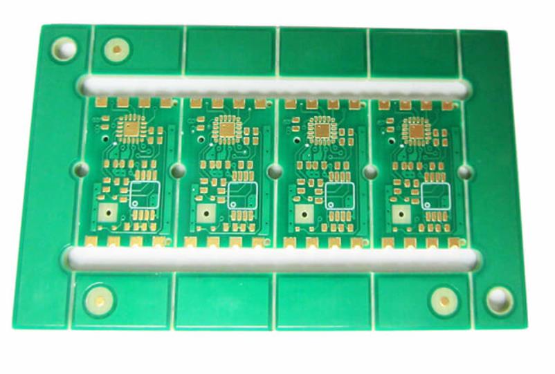
Payload weight has a direct influence on drone flight endurance, operating range, and energy consumption. A heavier surveillance payload can increase power consumption and reduce the amount of time the drone can remain in the air.
Security and surveillance systems may need to integrate multiple components, including high-resolution cameras, infrared sensors, wireless communication modules, image processors, storage devices, and navigation electronics.
Therefore, reducing the weight of every electronic component can help optimize the overall payload.
A Drone PCB should use an efficient structure that minimizes unnecessary material and occupied space while maintaining sufficient mechanical strength. Compact board dimensions, optimized layer structures, and appropriate material selection can help reduce PCB weight without compromising essential electrical functions.
This is particularly valuable for drones used in large-area surveillance applications where long flight times and extended operating ranges are important.
Drone surveillance equipment can operate in demanding outdoor environments. During flight, electronic systems may experience vibration, mechanical shock, temperature changes, wind, dust, humidity, and other environmental stresses.
The PCB serves as the electrical interconnection platform for cameras, sensors, processors, communication modules, and other electronic components. Therefore, it must maintain stable electrical connections even when the drone is continuously moving or experiencing vibration.
PCB material selection, layer bonding, mechanical structure, soldering quality, and manufacturing accuracy all contribute to the reliability of the finished board.
For outdoor security applications, the PCB manufacturing process should therefore consider not only electrical performance but also mechanical stability and environmental durability.
Modern drone surveillance systems are moving beyond basic image capture and wireless transmission. Advanced platforms can integrate functions such as intelligent image analysis, target recognition, thermal imaging, real-time data processing, and automated warning systems.
These additional functions increase the number of electronic components and interconnections required within the same physical space.
As a result, PCB designers need to achieve higher circuit density while maintaining reliable signal transmission.
For applications requiring advanced fabrication technology, HDI PCB technology can provide additional routing capacity within a compact board area. Microvias, blind vias, buried vias, and sequential build-up structures can help improve interconnection density and support smaller electronic assemblies.
GOPCBA provides HDI PCB Manufacturing solutions for high-density electronic designs where conventional through-hole structures may not provide sufficient routing flexibility.
Drone surveillance systems used for long-term outdoor operations require practical maintenance solutions. Electronic modules may need to be inspected, repaired, or replaced during the service life of the equipment.
A compact and lightweight PCB can simplify the mechanical integration of the electronic module. At the same time, appropriate board dimensions, mounting structures, connector placement, and component arrangement can make the system easier to service.
Reliable manufacturing quality is equally important because PCB defects can result in unexpected equipment downtime and increase maintenance costs.
The manufacturing process of a lightweight PCB should translate the application requirements into practical design and production solutions. Material selection, circuit density, board structure, drilling, lamination, and inspection all influence the final performance of the board.
Weight reduction starts with the selection of suitable PCB materials and board structures.
A lightweight board can use thinner construction and optimized layer configurations when the electrical and mechanical requirements of the application allow it. The objective is not simply to make the board thinner, but to achieve an appropriate balance between weight, rigidity, electrical performance, and manufacturing reliability.
For more complex electronic systems, a Multilayer PCB can provide additional routing and power-distribution layers within a relatively compact footprint.
GOPCBA provides Multilayer PCB Manufacturing capabilities for electronic products requiring higher circuit density, multiple signal layers, power planes, and complex interconnections.
Drone surveillance systems often need to accommodate a large number of electronic functions within a limited enclosure.
High-density routing allows more signal connections to be integrated into a smaller PCB area. However, increasing circuit density also requires tighter control of trace width, spacing, via dimensions, layer registration, and manufacturing tolerances.
The PCB stack-up must be designed according to the actual electrical requirements of the system.
For high-speed cameras, wireless communication modules, processors, and other data-intensive circuits, signal integrity should also be considered during the PCB design and manufacturing stages.
GOPCBA’s PCB Manufacturing Services support advanced PCB structures, including multilayer, HDI, high-speed, high-frequency, rigid-flex, heavy-copper, and controlled-impedance boards. This allows PCB construction to be matched more closely to the requirements of different drone electronic systems.
Although lightweight construction is important, reducing weight cannot come at the expense of reliability.
During flight, the PCB can experience continuous vibration and occasional mechanical shock. The board structure therefore needs sufficient mechanical stability to maintain reliable electrical connections.
Manufacturing parameters such as lamination quality, drilling accuracy, copper plating, solder mask application, and surface finishing all influence the reliability of the finished PCB.
For outdoor surveillance systems, appropriate material selection and manufacturing control can help the PCB maintain stable performance over a wide range of operating conditions.
Compact PCB designs require accurate manufacturing because small dimensional deviations can become more significant as trace spacing and component pitch decrease.
Important manufacturing parameters include:
- Trace width and spacing
- Via diameter
- Pad dimensions
- Layer-to-layer registration
- Board thickness
- Copper thickness
- Solder mask registration
- Overall board dimensions
GOPCBA provides detailed PCB Manufacturing Capabilities covering standard and advanced PCB structures, including HDI features, microvias, copper-filled microvias, buried vias, and tight dimensional requirements.
High-resolution cameras generate large amounts of image data and require reliable electrical connections between image sensors, processors, storage devices, and communication modules.
A compact PCB can help integrate these functions into a lightweight camera system while minimizing the space occupied inside the drone payload.
Infrared and thermal imaging technologies are widely used for nighttime surveillance, perimeter monitoring, search operations, and security applications.
These systems may require dedicated sensor interfaces, signal processing circuits, power management, and communication functions. PCB design must therefore provide sufficient routing density while maintaining stable signal transmission.
Real-time surveillance requires the transmission of images, video, control signals, and sensor information between the drone and the ground station.
Communication circuits can be sensitive to electromagnetic interference and signal integrity problems. Proper PCB stack-up, grounding, routing, and impedance control can help support reliable high-speed communication.
Modern drones increasingly incorporate onboard processing for functions such as target detection, object recognition, tracking, and intelligent alerts.
These applications can require processors, memory, storage, sensors, and communication interfaces to operate simultaneously within a limited physical space.
High-density PCB technologies provide an effective foundation for integrating these functions into compact electronic modules.
For security and surveillance equipment, PCB quality directly affects system stability. A circuit board failure can interrupt image transmission, sensor operation, communication, or control functions.
A comprehensive quality management process should therefore cover material inspection, manufacturing process control, dimensional inspection, electrical testing, and final product verification.
Typical inspection processes may include:
- Automated optical inspection
- Dimensional inspection
- Copper thickness verification
- Electrical testing
- Solder mask inspection
- Surface finish inspection
- X-ray inspection where required
- Final visual inspection
GOPCBA’s PCB Quality Management system includes incoming material control, manufacturing process control, electrical testing, technical review, and quality inspection to support consistent PCB production.
Quality control should begin before fabrication. Engineering review can identify potential manufacturing risks related to board thickness, trace spacing, via structures, layer stack-up, and material selection.
When developing a PCB for drone security equipment, engineers should evaluate the entire electronic system rather than focusing only on board weight.
Important considerations include:
Weight
The PCB should be optimized to reduce unnecessary weight while maintaining sufficient mechanical strength.
Board Size
The PCB dimensions should match the available installation space and the mechanical structure of the drone or surveillance module.
Circuit Density
High-density routing may be required when multiple sensors, processors, communication interfaces, and power circuits must be integrated into a compact area.
Signal Integrity
High-speed image data and wireless communication signals require appropriate routing, grounding, and stack-up design.
Thermal Management
Processors, communication modules, power devices, and other components may generate heat. The PCB structure should provide appropriate thermal paths according to the application.
Mechanical Reliability
The PCB should be capable of withstanding vibration and mechanical stress during flight.
Manufacturing Feasibility
The design must remain within the capabilities of the selected PCB manufacturer. Trace spacing, via size, layer registration, material thickness, and other parameters should be evaluated before production.
As drone surveillance systems continue to become more intelligent and multifunctional, PCB requirements will continue to evolve.

- Lower PCB weight
- Higher circuit density
- Smaller form factors
- Faster signal transmission
- Improved thermal management
- Greater environmental reliability
- Advanced HDI structures
- Higher integration of sensing and processing functions
The challenge is not simply to reduce PCB size and weight. Instead, manufacturers need to achieve an appropriate balance between lightweight construction, electrical performance, mechanical reliability, thermal behavior, and manufacturing feasibility.
For increasingly compact drone platforms, advanced multilayer and HDI technologies can provide greater design flexibility and help integrate more electronic functions into smaller spaces.
Lightweight PCB technology plays an important role in the development of drone security and surveillance equipment. By combining lightweight construction, compact dimensions, high-density routing, reliable materials, and precise manufacturing processes, PCBs can help drone systems achieve better payload efficiency while maintaining stable electronic performance.
As surveillance drones incorporate higher-resolution imaging, infrared sensing, intelligent processing, wireless communication, and automated analysis, PCB requirements will become increasingly demanding.
A successful PCB solution must therefore consider the complete application environment—from weight and mechanical constraints to signal integrity, thermal management, manufacturing accuracy, and quality control.
With appropriate PCB design and manufacturing technologies, lightweight circuit boards can provide a reliable electronic foundation for next-generation drone security, surveillance, and monitoring systems.