Heavy Copper PCB Manufacturing for High-Power Electronics
Reliable printed circuit boards are fundamental to modern power electronics. Power supplies, industrial controllers, battery systems, motor drives, renewable energy equipment, and other high-load applications place significantly greater demands on PCB current capacity, heat dissipation, mechanical strength, and long-term reliability than conventional electronic products.
For these applications, Heavy Copper PCB technology provides an effective way to increase conductor cross-sectional area, reduce electrical resistance, improve current-carrying capability, and enhance thermal performance. However, successful heavy copper manufacturing requires much more than simply increasing the copper weight. Material selection, stack-up design, copper distribution, etching, plating, drilling, lamination, thermal management, and electrical testing must all be considered as part of an integrated manufacturing process.
GOPCBA provides customized PCB manufacturing solutions for demanding power applications, supporting different board structures, copper thicknesses, materials, and production requirements.
Why Heavy Copper PCB Technology Matters for Power Electronics
A conventional PCB may be sufficient for low- and medium-power electronic circuits. As current increases, however, narrow copper traces can experience higher resistance, voltage drop, and temperature rise.
A Power PCB is designed around the electrical and thermal requirements of the application. Depending on the circuit, the design may incorporate thicker copper layers, wider conductors, large copper planes, thermal vias, reinforced connections, or specialized materials.
Heavy Copper PCB Manufacturing can be particularly valuable when conventional copper thickness cannot provide the required current capacity or thermal performance.
Higher Current-Carrying Capability
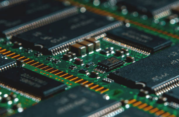
Copper thickness directly affects the cross-sectional area available for current flow. Increasing copper thickness can reduce conductor resistance and support higher current loads when combined with appropriate trace width and thermal conditions.
This makes heavy copper technology suitable for applications such as:
- Power supplies
- DC-DC converters
- AC-DC power systems
- Battery management systems
- Motor controllers
- Inverters
- Industrial power equipment
- Renewable energy systems
- Automotive power electronics
- High-current control systems
The appropriate copper weight should always be determined according to current requirements, allowable temperature rise, trace geometry, layer structure, and manufacturing capability.
Lower Electrical Losses
Higher copper cross-sectional area can reduce conductor resistance and therefore reduce I²R losses in high-current paths.
Potential benefits include:
- Lower voltage drop
- Reduced conductor heating
- Improved electrical efficiency
- More stable high-load operation
- Better thermal distribution
For continuous-load power systems, controlling conductor losses can have a significant effect on overall system efficiency and thermal performance.
Material Selection for High-Power PCB Manufacturing
Material selection is another important factor in reliable Power Electronics PCB production.
FR-4 remains widely used for many power applications, while high-Tg FR-4 and other specialized materials may be selected when the design requires improved thermal stability, dimensional stability, or other electrical characteristics.
The correct material depends on the operating temperature, voltage, current, board thickness, dielectric requirements, thermal environment, and expected service conditions.
For complex designs, the material should be evaluated together with the copper structure and complete stack-up rather than selected independently.
Copper Weight and Layer Configuration
Heavy copper can be applied to external layers, internal layers, or selected power layers depending on the circuit architecture.
Common design considerations include:
- Copper weight
- Number of layers
- Dielectric thickness
- Board thickness
- Current distribution
- Thermal requirements
- Mechanical requirements
- Manufacturing tolerances
For example, a multilayer board can separate power, ground, and signal functions while providing dedicated copper areas for high-current paths.
For complex stack-ups, PCB Manufacturing Services can support different PCB structures and manufacturing requirements from prototype development through production.
Thermal Management Is Critical for High-Current PCBs
Electrical performance and thermal performance are closely connected in high-power circuit boards.
High current produces heat through conductor resistance, while power components such as MOSFETs, IGBTs, regulators, transformers, and power modules can generate significant localized heat.
A properly engineered High-Current PCB should therefore provide a controlled thermal path from heat-generating components to the PCB copper structure and, where applicable, to external heat-dissipation components.
Large Copper Areas
Large copper pours and planes can spread heat over a larger area and reduce localized temperature concentration.
They can also provide lower-resistance current paths for power distribution.
Thermal Vias
Thermal vias provide conductive paths between component pads, copper layers, and heat-spreading structures.
Depending on the design, engineers may use:
- Multiple thermal vias
- Via arrays
- Larger current-carrying vias
- Copper-filled vias
- Dedicated thermal layers
The appropriate via structure depends on current, thermal resistance, component package, PCB thickness, and manufacturing limitations.
Embedded Copper Structures
For applications with particularly demanding thermal requirements, embedded copper coins or other internal copper structures can provide a more direct thermal path.
This approach can be useful when conventional thermal vias and copper planes alone cannot provide sufficient heat transfer.
The final thermal structure should be evaluated according to component power dissipation, thermal resistance, PCB construction, and the available cooling system.
Manufacturing Challenges of Heavy Copper PCBs
Manufacturing heavy copper boards is more demanding than producing conventional PCBs.
Increasing copper thickness affects several fabrication processes, including imaging, etching, electroplating, drilling, lamination, solder mask application, and dimensional control.
Etching and Line Definition
Thicker copper requires careful control of the etching process.
As copper thickness increases, maintaining accurate line width and spacing becomes more challenging. The manufacturing process must compensate for etching characteristics while maintaining the required circuit geometry.
This is especially important when a board combines heavy copper power circuits with relatively fine signal routing.
Copper Plating
Copper plating must provide reliable conductivity and adequate coverage throughout the board.
Special attention may be required around plated through-holes, vias, corners, and other high-stress structures.
Plating thickness, current distribution, bath control, and process consistency all influence the final board quality.
Lamination and Thermal Expansion
Heavy copper structures can influence heat distribution and dimensional behavior during lamination.
A controlled lamination process helps manage:
- Resin flow
- Layer alignment
- Board thickness
- Internal stress
- Thermal expansion
- Potential warpage
The copper distribution across the board should also be considered during stack-up development to maintain manufacturing stability.
Quality Control for High-Reliability Power PCBs
A high-power circuit board must maintain consistent electrical and mechanical performance throughout production.
Quality control should therefore cover raw materials, manufacturing processes, dimensional characteristics, copper structures, electrical performance, and final inspection.
A High-Reliability PCB manufacturing workflow may include:
Automated Optical Inspection
AOI can identify visible circuit-pattern defects such as opens, shorts, missing copper, dimensional deviations, and other abnormalities.
Electrical Testing
Electrical testing can verify circuit continuity and isolation, helping detect open circuits and short circuits before shipment.
Copper and Hole Inspection
Copper thickness, plated-hole characteristics, hole dimensions, and critical structures should be verified against the approved specifications.
Thermal and Reliability Testing
Depending on the application, additional reliability testing may include thermal shock, thermal cycling, solderability, dielectric withstand, insulation resistance, or other customer-defined tests.
The specific test method and acceptance criteria should be determined according to the PCB design and end-use requirements.
From PCB Fabrication to PCBA
Power PCB performance does not end with bare-board fabrication. Component selection, soldering, thermal interfaces, mechanical mounting, and assembly quality can also affect system reliability.
For power electronics, assembly processes may need to accommodate:
- Large copper areas
- High-power components
- Large thermal pads
- Through-hole power devices
- Mixed SMT and THT components
- Heat sinks
- Thermal interface structures
GOPCBA supports PCB fabrication and assembly requirements for different circuit structures. PCB Assembly Services can help integrate bare-board manufacturing with component assembly and production engineering.
This integrated approach can reduce manufacturing handoffs and allow fabrication and assembly requirements to be reviewed together.
Applications of Heavy Copper and Power PCBs
Heavy copper and high-current PCB technologies are widely applicable to electronic systems where current density, thermal performance, and reliability are critical.
Industrial Power Systems
Industrial power supplies, motor controls, automation equipment, and power conversion systems often require robust current paths and reliable thermal management.
Battery and Energy Storage Systems
Battery systems can involve high-current charging and discharging paths. PCB designs may therefore require larger copper areas, appropriate thermal structures, and carefully engineered power distribution.
Renewable Energy Equipment
Solar power converters, energy storage systems, inverters, and other renewable energy equipment can benefit from PCB structures designed for continuous electrical loads and thermal stress.
Automotive Power Electronics
Electric vehicles and modern automotive systems increasingly depend on power electronics for battery management, charging, motor control, and power conversion.
In these applications, heavy copper may be selected when the electrical and thermal requirements justify the additional manufacturing complexity.
Telecommunications and Industrial Equipment
High-power communication equipment and industrial control systems may also require reliable power distribution and heat management within compact PCB assemblies.
Why Engineering Review Should Start Before Manufacturing
Heavy copper requirements should not be added after the PCB layout is completed.
The copper weight, trace width, layer stack-up, via structure, component placement, thermal path, board thickness, and manufacturing tolerances should be evaluated during the engineering stage.
Early DFM analysis can help identify potential problems such as:
- Excessive copper imbalance
- Difficult etching structures
- Insufficient via capacity
- Thermal concentration
- Lamination risks
- Manufacturing tolerance conflicts
- Inadequate creepage or clearance
- Assembly-related thermal problems
For more complex power designs, early engineering review can reduce unnecessary redesigns and improve production consistency.
Building a Reliable Power PCB Manufacturing Strategy
A reliable power PCB is the result of coordinated electrical, thermal, mechanical, and manufacturing engineering.
Simply increasing copper thickness does not automatically produce a better PCB. The final design must balance current capacity, thermal performance, signal requirements, manufacturability, reliability, and cost.
GOPCBA provides manufacturing support for heavy copper, multilayer, high-Tg, high-frequency, rigid-flex, HDI, controlled-impedance, and other customized PCB technologies. PCB Capabilities
For high-power applications, the manufacturing strategy can be developed around the actual requirements of the end product, including copper weight, stack-up, material selection, thermal design, inspection, and assembly.
Conclusion
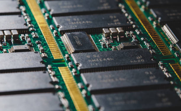
As power electronics continue to become more compact and powerful, PCB technology must provide reliable current transmission, effective heat dissipation, and stable long-term performance.
Heavy Copper PCB technology offers an effective solution for high-current applications by increasing copper cross-sectional area and supporting improved electrical and thermal performance. However, reliable results depend on the complete manufacturing process, including material selection, stack-up engineering, etching, plating, lamination, drilling, thermal design, inspection, and testing.
For demanding applications, a well-engineered Power PCB should be developed around the actual electrical and thermal requirements rather than relying on a one-size-fits-all construction.
With appropriate engineering analysis and manufacturing process control, heavy copper and high-current PCB technologies can provide a strong foundation for reliable power supplies, industrial systems, energy equipment, automotive electronics, and other high-power applications.