Precision PCB Drilling for Microvias and High-Density Interconnects
As electronic products become smaller, faster, and more highly integrated, PCB manufacturers face increasing challenges in fitting more electrical connections into limited board space. Conventional through-hole structures can consume significant routing area, making it difficult to achieve the density required by modern communication equipment, computing systems, automotive electronics, medical devices, and compact industrial products.
This is where Precision PCB Drilling and high-density interconnect technology become increasingly important.
Advanced PCB fabrication can use mechanical drilling, laser drilling, microvias, blind vias, buried vias, and sequential buildup structures to create efficient interlayer connections. These technologies allow engineers to shorten electrical paths, increase routing density, support fine-pitch components, and optimize PCB dimensions without simply increasing the physical size of the board.
However, smaller holes do not automatically mean better performance. Hole diameter, aspect ratio, drill accuracy, copper plating, layer registration, dielectric structure, via reliability, and the overall PCB stack-up must be considered together.
Why Precision PCB Drilling Matters in Modern PCB Manufacturing
PCB drilling creates the physical structures required for electrical connections between different circuit layers.
In conventional multilayer boards, mechanical through-holes can connect multiple layers. As routing density increases, however, these vias may occupy valuable space across the entire board.
Precision drilling provides alternative structures that use space more efficiently.
Depending on the design, manufacturers may use:
- Mechanical through-holes
- Laser-drilled microvias
- Blind vias
- Buried vias
- Stacked microvias
- Staggered microvias
- Via-in-pad structures
The appropriate structure depends on PCB layer count, component pitch, routing density, electrical requirements, material characteristics, and manufacturing capability.
For projects requiring advanced fabrication, GOPCBA publishes capabilities covering conventional multilayer structures as well as HDI and microvia technologies. Its PCB Capabilities include HDI microvias, stacked microvias, copper-filled microvias, buried vias, and advanced buildup structures.
What Are Microvias?
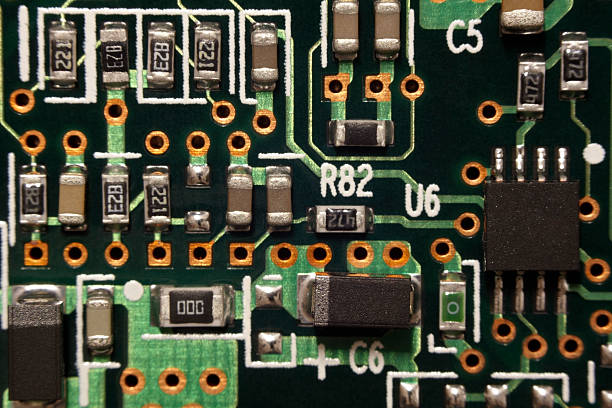
A Microvia PCB uses very small laser-drilled vias to establish connections between selected PCB layers.
Unlike a conventional through-hole via that may pass through the complete board, a microvia generally connects adjacent or nearby layers within an HDI buildup structure.
This difference provides an important routing advantage.
Smaller Vias Save Routing Space
A conventional through-hole consumes routing space through multiple layers. A microvia can connect only the layers required by the circuit, leaving more available routing channels on other layers.
This can be particularly valuable around:
- Fine-pitch BGAs
- High-density IC packages
- Compact processors
- Memory devices
- High-speed interfaces
- RF components
- Miniaturized electronic modules
Microvias can therefore help designers achieve greater circuit density without continuously increasing PCB dimensions.
Laser Drilling for Microvia Formation
Microvias are commonly produced using laser drilling rather than conventional mechanical drilling.
Laser drilling provides the dimensional control required for small via structures, but the actual manufacturable minimum depends on the material system, copper thickness, dielectric construction, laser process, aspect ratio, and manufacturer capability.
For example, GOPCBA’s published HDI capability lists standard microvia holes down to 100 μm and advanced capability down to 75 μm. These values should be treated as manufacturer capability references rather than universal PCB design rules.
HDI PCB Manufacturing and High-Density Interconnects
HDI PCB technology extends the advantages of microvias into a complete high-density interconnection architecture.
HDI boards typically combine fine-line routing, microvias, blind vias, buried vias, and sequential buildup processes to increase routing density.
The objective is not simply to make every feature smaller. Instead, HDI technology provides more efficient interconnections between components and PCB layers.
A typical HDI structure may include:
- Core multilayer construction
- Buildup dielectric layers
- Laser-drilled microvias
- Blind vias
- Buried vias
- Fine-line circuitry
- Sequential lamination
- Copper-filled microvias
The exact construction depends on the electrical and mechanical requirements of the product.
For a deeper look at practical HDI structures, HDI PCB Design Rules explains microvia structures, blind and buried vias, sequential buildup, routing density, and manufacturability considerations.
Blind Vias vs. Buried Vias vs. Microvias
Understanding the differences between via structures is essential when developing a high-density PCB.
Blind Vias
A blind via connects an outer PCB layer to one or more internal layers without extending through the entire board.
This structure can save routing space and is commonly used for:
- BGA escape routing
- Fine-pitch components
- HDI buildup layers
- High-density interconnections
Buried Vias
A buried via is located entirely inside the PCB structure and connects internal layers without reaching either external surface.
Because it does not occupy the outer layers, a buried via can provide additional internal routing flexibility.
However, buried vias generally require additional manufacturing processes, so they should be used when the routing or electrical benefits justify the added fabrication complexity.
Microvias
Microvias are small laser-drilled structures commonly associated with HDI manufacturing.
They can be arranged as:
- Staggered microvias
- Stacked microvias
- Copper-filled microvias
Staggered microvias offset adjacent vias between buildup layers and can offer manufacturing advantages.
Stacked microvias are vertically aligned and can provide very high routing efficiency, but they require tighter process control.
GOPCBA’s published capabilities support both stacked and copper-filled microvias for advanced HDI structures.
How Precision Drilling Supports High-Density Routing
The primary value of precision drilling is not simply the size of the hole. It is the ability to create predictable interlayer connections that work within a highly constrained PCB layout.
A smaller and accurately positioned via can provide several benefits.
More Routing Channels
Reducing via dimensions can free additional space for traces and component escape routing.
This is especially important around high-pin-count components where hundreds or thousands of connections may need to exit a small package area.
Shorter Electrical Connections
Microvias can connect adjacent layers directly instead of forcing signals through a full-board through-hole structure.
Shorter connections can help reduce unnecessary routing length and may improve electrical performance when combined with an appropriate stack-up and signal-integrity strategy.
Smaller PCB Dimensions
Higher interconnection density can allow designers to reduce board area while maintaining the required number of electrical connections.
This is particularly valuable for compact devices where PCB size is constrained by the mechanical enclosure.
Precision Drilling Process Control
Reliable PCB Drilling Technology requires precise control throughout the drilling process.
The required parameters depend on whether the board uses mechanical holes, laser microvias, blind vias, buried vias, or more advanced via structures.
Material and Stack-Up Analysis
Before drilling begins, engineers must understand the PCB material system and complete stack-up.
Important factors include:
- Dielectric thickness
- Copper thickness
- Material composition
- Layer count
- Finished board thickness
- Via diameter
- Aspect ratio
- Required interlayer connection
The drilling process must be compatible with the physical structure of the PCB.
Drill Position Accuracy
Via position must correspond accurately with the circuit pattern and pad locations.
Registration errors can become increasingly significant as feature sizes decrease. This makes alignment between imaging, drilling, lamination, and plating processes essential.
Hole-Wall Quality
After drilling, the hole wall must be suitable for subsequent copper deposition.
Mechanical drilling can generate burrs and debris, while laser drilling requires controlled removal of dielectric material and appropriate treatment of the resulting structure.
The subsequent desmear, activation, and plating processes must establish a reliable conductive path.
Copper Plating and Via Reliability
Drilling alone does not create a finished electrical connection. The drilled structure must be properly metallized.
Copper plating establishes conductivity between PCB layers and must provide appropriate coverage throughout the hole or via structure.
For advanced HDI boards, via filling may also be required.
Copper-filled or resin-filled structures can provide a planar surface and support subsequent buildup or component assembly processes.
GOPCBA’s recent manufacturing guidance highlights that via plugging and filling require control of filling quality, voids, adhesion, curing, planarization, and subsequent plating compatibility.
For high-reliability applications, via quality should therefore be evaluated as part of the complete PCB manufacturing process rather than as an isolated drilling operation.
Precision Drilling and Signal Integrity
As data rates increase, via structures can become part of the electrical transmission path.
A poorly designed or poorly controlled via transition may introduce impedance discontinuities, reflections, parasitic effects, or unwanted coupling.
For High-Density Interconnect PCB designs carrying high-speed signals, engineers should evaluate:
- Via geometry
- Stub length
- Layer transitions
- Reference planes
- Return-current paths
- Differential-pair transitions
- Impedance
- Crosstalk
- Material properties
High-speed PCB manufacturing therefore requires coordination between PCB layout and fabrication.
GOPCBA’s High-Speed PCB Manufacturing guidance emphasizes that manufacturing variables such as trace geometry, dielectric thickness, via structures, layer registration, materials, and stack-up can directly influence signal integrity.
Microvias and Fine-Pitch Component Routing
Fine-pitch components create a significant routing challenge because many electrical connections must escape from a very small footprint.
Traditional through-hole vias may occupy too much space beneath or around the component.
Microvias can provide a more compact escape structure.
BGA Applications
BGA packages are a common application for HDI microvias.
Depending on the package pitch and PCB structure, microvias can be positioned within or near component pads to create shorter escape routes.
Via-in-pad technology can further improve routing efficiency, although it requires appropriate filling, planarization, and manufacturing controls.
The decision to use via-in-pad should therefore be based on the component package, assembly process, reliability requirements, and PCB manufacturer’s process capability.
Sequential Lamination for HDI PCBs
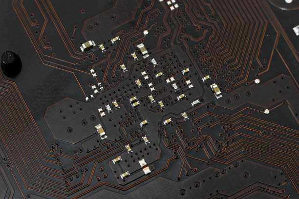
Advanced HDI structures frequently require sequential buildup.
Instead of manufacturing the entire multilayer board in one conventional lamination cycle, buildup layers can be added in stages.
A simplified process may involve:
- Manufacturing the core structure
- Adding dielectric buildup material
- Laser drilling microvias
- Copper deposition and plating
- Circuit formation
- Additional lamination
- Repeating the buildup process as required
- Final surface processing and inspection
The exact sequence depends on the HDI structure, such as 1+N+1, 2+N+2, or more advanced configurations.
Sequential lamination requires careful control of layer registration, material thickness, thermal behavior, and via alignment.
Manufacturing Inspection for Precision PCB Drilling
As PCB features become smaller, inspection becomes increasingly important.
A comprehensive quality-control process may include:
Dimensional Inspection
Hole diameter, pad dimensions, board dimensions, and critical geometries can be verified against manufacturing requirements.
AOI
Automated optical inspection can detect circuit-pattern defects and other visible abnormalities after imaging and etching.
Cross-Section Analysis
Cross-sectional analysis can provide detailed information about:
- Hole-wall structure
- Copper thickness
- Via filling
- Layer alignment
- Dielectric thickness
- Internal defects
This type of analysis is particularly useful for verifying advanced PCB structures.
Electrical Testing
Electrical testing can identify opens and shorts and verify electrical continuity.
For high-density boards, electrical testing complements physical inspection by confirming that the intended interconnections are electrically functional.
Applications of Precision Drilled and HDI PCBs
Precision drilling and HDI manufacturing are used across many advanced electronics applications.
Smartphones and Portable Electronics
Compact consumer electronics require high routing density within limited PCB dimensions. Microvias and fine-line structures can help accommodate dense component packages.
Automotive Electronics
Automotive control modules, communication systems, ADAS electronics, and compact sensor modules can benefit from HDI structures where routing density and package integration are important.
Medical Electronics
Portable and compact medical devices may require dense interconnection structures to integrate processors, sensors, communication interfaces, and power-management circuits.
Telecommunications
Communication equipment often combines high-speed digital circuits with dense component placement. HDI and precision via structures can support compact layouts while maintaining controlled electrical paths.
High-Performance Computing
AI servers, processors, networking equipment, and other computing platforms increasingly require high layer counts, high-density routing, and advanced signal-integrity management.
Precision Drilling Is a Complete Manufacturing Discipline
It is tempting to evaluate PCB drilling simply by asking how small a hole a manufacturer can produce.
In practice, that is only one part of the capability.
A reliable precision-drilled PCB depends on the interaction between:
- PCB material
- Stack-up
- Copper thickness
- Drill technology
- Laser parameters
- Hole-wall treatment
- Plating
- Via filling
- Layer registration
- Circuit geometry
- Inspection
- Electrical testing
A manufacturer may be capable of producing very small holes, but the more important question is whether those structures can be manufactured consistently and integrated reliably into the complete PCB process.
GOPCBA’s broader PCB Manufacturing capabilities cover multilayer, HDI, high-speed, controlled-impedance, blind and buried via, rigid-flex, and heavy copper PCB fabrication.
How to Choose the Right PCB Drilling Solution
The appropriate drilling method should be selected according to the actual electrical and mechanical requirements of the board.
Consider the following factors before finalizing the design:
- Required hole diameter – Determine whether mechanical drilling or laser drilling is appropriate.
- Layer connectivity – Decide whether through, blind, buried, or microvia structures are required.
- Routing density – Evaluate whether conventional vias provide enough routing space.
- Component pitch – Fine-pitch packages may require HDI structures.
- Signal speed – High-speed signals require careful via and stack-up analysis.
- Board thickness – Consider aspect ratio and drilling feasibility.
- Reliability requirements – Evaluate thermal cycling, mechanical stress, and expected service conditions.
- Manufacturing capability – Confirm the fabricator’s actual minimum feature and via specifications before layout.
This engineering-first approach helps prevent designs that are theoretically possible but difficult or expensive to manufacture consistently.
Conclusion
As electronic products continue to become smaller and more powerful, conventional PCB interconnection methods are increasingly challenged by limited board space and rising routing density.
Precision PCB Drilling provides the foundation for advanced interconnection structures, while microvias, blind vias, buried vias, and sequential buildup extend these capabilities into modern HDI manufacturing.
The value of these technologies goes beyond smaller holes. Properly engineered via structures can increase routing density, shorten electrical paths, support fine-pitch components, improve space utilization, and provide greater flexibility for compact high-performance PCB designs.
At the same time, precision drilling must be integrated with material selection, stack-up design, lamination, copper plating, via filling, layer registration, signal-integrity analysis, inspection, and electrical testing.
For advanced electronics, the goal should not simply be to achieve the smallest possible hole. The real objective is to create a Microvia PCB or HDI PCB structure that can be manufactured consistently, tested reliably, and integrated into the complete electronic system.
When precision drilling is treated as part of a complete engineering and manufacturing strategy, it becomes a powerful technology for supporting the next generation of high-density, miniaturized, and high-performance electronics.