Through Hole PCB Vs Blind Via vs Buried Via PCB A Complete Guide to Understanding PCB Vias
In PCB structures, different types of vias are used to connect circuits between layers and ensure reliable signal transmission. Among them, through hole PCB, blind via PCB, and buried via PCB are three of the most common technologies.
Because they all serve the purpose of electrical connection, many people often confuse their differences. However, by understanding their basic structures, connection methods, and application scenarios, these three via types can be easily distinguished.
This article explains the differences between through holes, blind vias, and buried vias from four aspects: definitions, key differences, applications, and identification methods.
1. Understanding the Basic Definitions of Three PCB Via Types
To distinguish different via structures, the first step is understanding their depth and connection range inside the PCB.
Through Hole: A Via That Passes Through the Entire PCB
A through hole extends completely from the top surface of the PCB to the bottom surface.
Regardless of the number of PCB layers, a through hole can connect the outermost layers and may also connect internal layers along its path.
From the outside, openings can be seen on both the top and bottom sides of the circuit board.
The main characteristics of through holes include:
- Passes through the entire PCB thickness
- Visible from both sides
- Simple manufacturing process
- Suitable for many conventional PCB applications
Because of its mature technology and relatively low manufacturing cost, through holes remain widely used in standard circuit boards.
For more information about PCB manufacturing capabilities, explore our PCB fabrication services.
Blind Via: Connecting the Surface Layer to an Internal Layer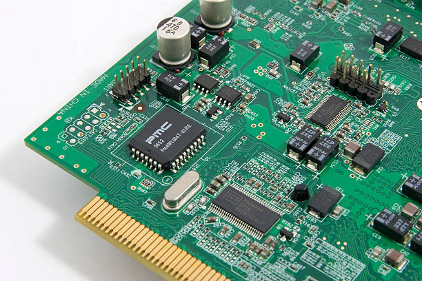
A blind via does not pass through the entire PCB.
Instead, it starts from one external surface of the PCB and extends only to a specific internal layer before stopping.
For example, a blind via may start from the top layer and connect to the second layer, but it will not continue through to the bottom surface.
The characteristics of blind vias include:
- Visible opening on only one PCB surface
- Connects an outer layer with an internal layer
- Does not occupy the entire board thickness
- Helps increase routing density
Blind vias are commonly used in high-density PCB designs where space is limited.
Buried Via: Hidden Connections Inside the PCB
A buried via is completely located inside the PCB structure.
It does not extend to the top or bottom surface. Instead, it connects only internal layers of the PCB.
For example, in a four-layer PCB, a buried via may connect the second layer and the third layer without appearing on either external surface.
The characteristics of buried vias include:
- Invisible from both PCB surfaces
- Located entirely inside the board
- Used for internal layer connections
- Supports high-density PCB structures
Because buried vias require more complex manufacturing processes, they are usually applied in advanced multilayer PCB designs.
Learn more about our multilayer PCB manufacturing solutions for complex PCB structures.
2. Key Differences: Identify Them Through Visibility and Connection Range
Besides their definitions, the easiest way to distinguish these three via types is by analyzing visibility and layer connection range.
Visibility: Can the Via Opening Be Seen?
Through Hole
A through hole can be seen from both the top and bottom surfaces.
It is considered a:
Double-sided visible via
Blind Via
A blind via can only be seen from the surface where drilling begins.
It is considered a:
Single-sided visible via
Buried Via
A buried via cannot be seen from either external surface.
It is considered a:
Invisible internal via
Connection Range: Which Layers Can Be Connected?
Through Hole
Through holes provide the widest connection range.
They can connect:
- Top layer
- Bottom layer
- Multiple internal layers along the drilling path
Blind Via
Blind vias have a limited connection range.
They connect:
- External surface layer
- One or more internal layers
However, they cannot directly connect both external surfaces.
Buried Via
Buried vias only connect internal layers.
They connect:
- Internal layer to internal layer
They do not connect with external PCB surfaces.
3. Application Scenarios: Choosing the Right Via Technology
Different PCB designs require different via structures. Choosing the appropriate technology depends on product size, circuit complexity, and performance requirements.
Through Hole Applications
Through holes are widely used because they are simple, reliable, and cost-effective.
Typical applications include:
- Household appliances
- Industrial control boards
- Basic electronic devices
- General-purpose circuit boards
When PCB designs do not require extremely high wiring density, through-hole technology is often the most economical choice.
Blind Via Applications
Blind vias are mainly used in compact electronic products where PCB space is limited.
Common applications include:
- Smartphones
- Smart watches
- Portable electronic devices
- High-density circuit designs
Because blind vias do not pass through the entire board, they free up routing space on opposite layers and allow more compact component placement.
For advanced compact PCB designs, our HDI PCB manufacturing capabilities support high-density interconnection requirements.
Buried Via Applications
Buried vias are used when internal PCB layers require independent connections without affecting surface routing.
Typical applications include:
- Complex industrial control systems
- High-performance electronic equipment
- Advanced multilayer circuit boards
By keeping connections inside the PCB, buried vias help maximize surface space for components while improving routing flexibility.
They are especially valuable for high-layer-count PCB designs requiring compact and reliable electrical connections.
4. Practical Methods to Identify Different PCB Via Types
Understanding simple inspection methods can help quickly determine the type of via used on a PCB.
Method 1: Visual Inspection
Observe both the top and bottom surfaces of the PCB.
If openings are visible on both sides:
It is likely a through hole.
If an opening appears on only one side:
It may be a blind via.
If no opening is visible on either side:
It may be a buried via, although further verification is required.
Since buried vias are hidden inside the PCB structure, visual inspection alone cannot provide complete confirmation.
Method 2: Light Transmission Test
Use a flashlight or phone light to check the PCB.
If light passes through the board:
The via is likely a through hole.
If light appears only from one side:
The structure may be a blind via.
If no light transmission is visible from either side:
The PCB may contain buried vias, especially in high-layer-count boards.
Choosing the Right PCB Via Technology for Your Project
Through holes, blind vias, and buried vias each have unique advantages and application areas.
- Through hole PCB technology provides reliable connections with lower manufacturing costs.
- Blind via PCB technology improves routing density and supports compact electronic designs.
- Buried via PCB technology enables advanced internal layer connections for complex multilayer boards.
Selecting the right via structure depends on factors such as:
- PCB layer count
- Product size requirements
- Signal integrity requirements
- Manufacturing budget
- Circuit complexity
gopcba provides professional PCB manufacturing solutions, including advanced multilayer PCB technologies and high-density interconnection capabilities.
With experienced engineering support and optimized manufacturing processes, we help customers select the most suitable PCB structure to achieve reliable performance, efficient production, and competitive costs.