High Stability Image Processing PCB: Ensuring Reliable Performance for Advanced Imaging Applications
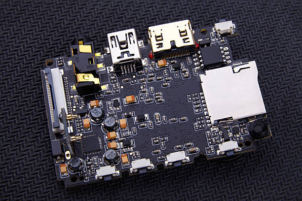
In modern imaging applications, from industrial vision inspection and medical imaging systems to security monitoring equipment, the demand for higher image quality and signal accuracy continues to increase. A high-performance Image Processing PCB serves as the critical foundation that ensures stable signal transmission from image acquisition to final output.
Unlike systems that rely heavily on external compensation technologies, a well-designed PCB structure can independently handle complex signal requirements, environmental variations, and high-speed data transmission challenges. By optimizing materials, circuit layout, thermal management, and reliability testing, advanced PCBs provide stable support for high-quality image processing systems.
For applications requiring complex circuit structures and enhanced signal integrity, Multilayer PCB technology provides additional routing layers, better electromagnetic control, and improved performance for high-density image processing systems.
Selecting PCB Materials for Image Processing Applications: Balancing Signal Integrity and Environmental Reliability
During image processing, signals typically operate at high speeds and across wide frequency ranges. These signals are highly sensitive to transmission delay, attenuation, and distortion. Meanwhile, many applications, such as industrial environments and medical equipment rooms, involve temperature fluctuations, humidity changes, and other external challenges.
Therefore, selecting the right PCB material is essential to achieving both stable signal transmission and strong environmental resistance.
The materials used in an advanced Image Processing PCB must provide excellent dielectric performance. A stable dielectric constant and low dielectric loss help minimize signal degradation during transmission.
For example, in 4K and 8K high-definition imaging systems, fluctuations in dielectric properties can cause signal timing errors, image edge distortion, or color inconsistency. In high-speed industrial vision systems, low-loss materials help maintain signal accuracy by reducing energy loss during transmission.
In addition to electrical performance, mechanical strength and thermal resistance are also critical. Industrial imaging equipment may experience vibration, temperature cycling, and long-term operation. If PCB materials lack sufficient durability, problems such as cracking, delamination, or signal interruption may occur.
Currently, many high-performance PCBs use reinforced epoxy resin combined with fiberglass materials to achieve a balance between electrical stability, mechanical strength, and environmental durability.
For more advanced PCB solutions, customers can explore our Custom PCB Manufacturing capabilities to achieve optimized designs for different imaging applications.
Solder Mask Protection: Creating a Barrier Against External Interference
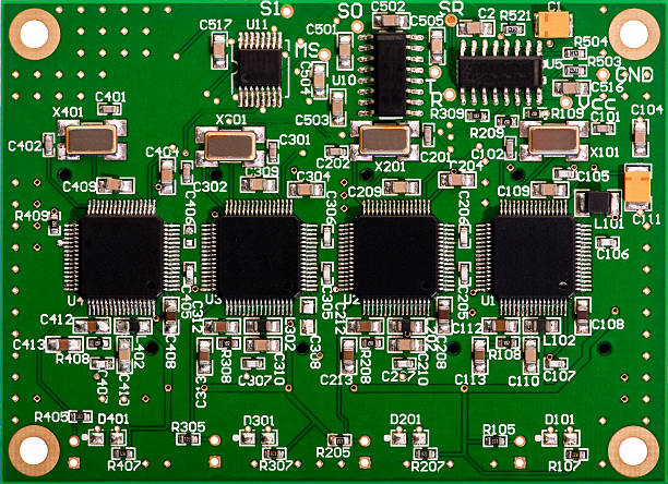
Surface protection plays an important role in maintaining long-term PCB reliability. The solder mask layer not only protects exposed copper circuits but also prevents contamination from dust, moisture, chemicals, and oxidation.
For an Image Processing PCB, the solder mask material must be selected according to the application environment.
For example, medical imaging equipment often operates in clean environments with controlled but relatively high humidity levels. In these conditions, the solder mask must provide excellent moisture resistance to prevent leakage currents and maintain stable image signal acquisition.
Outdoor security monitoring systems face additional challenges, including UV exposure, rain, and temperature changes. In these applications, the solder mask requires strong weather resistance to maintain protection throughout long-term operation.
Different solder mask colors are also used depending on application requirements. Black solder masks can absorb stray light and reduce optical interference in precision imaging equipment. This is particularly useful in systems where reflected light may affect sensor performance.
Green solder masks remain widely used because they provide balanced insulation performance, environmental resistance, and cost efficiency for industrial vision and medical imaging applications.
The coating quality of the solder mask is also critical. Uneven thickness, pinholes, or surface defects can become potential entry points for contamination and reduce overall PCB reliability.
Optimizing Signal Transmission Paths: Reducing Interference Through PCB Design
The signal routing structure inside an Image Processing PCB directly affects the quality and reliability of image data transmission.
A properly designed PCB layout ensures that signals travel efficiently from image sensors to processing chips and output interfaces while minimizing interference.
Short and Organized Signal Routing
One of the most important principles in high-speed PCB design is minimizing unnecessary routing length.
Long signal paths increase the risk of:
- Signal attenuation
- Electromagnetic interference
- Transmission delay
- Data distortion
Therefore, interfaces between image sensors, processors, and output connectors should be positioned strategically to reduce routing distance.
For example, in high-resolution camera systems, maintaining a short and direct connection between the image sensor and processing unit can significantly reduce signal loss and improve image accuracy.
Signal Isolation and Electromagnetic Control
Image processing boards contain different types of circuits, including:
- High-speed image signals
- Power supply lines
- Control signals
These circuits may interfere with each other if not properly separated.
A professional PCB layout uses techniques such as:
- Controlled spacing
- Ground plane optimization
- Differential pair routing
- Shielding structures
These methods reduce electromagnetic interference and ensure clean signal transmission.
For high-speed applications requiring strict signal control, our High Speed PCB solutions are designed to support demanding data transmission requirements.
Thermal Management: Maintaining Stable Operating Conditions
During image processing operations, processors and other electronic components generate significant heat. Without effective thermal management, excessive temperature increases can affect component performance and reduce image processing stability.
A reliable PCB design must include efficient heat dissipation methods to maintain consistent operating temperatures.
Thermal performance depends on several factors, including:
- PCB material thermal conductivity
- Copper thickness
- Heat dissipation structures
- Component placement
High thermal conductivity materials help transfer heat away from high-power components, preventing localized overheating.
For example, in advanced image processing systems, processors operating at high speeds may generate enough heat to reduce computing performance. A properly designed PCB can include larger copper areas, thermal vias, and connections to external cooling systems to improve heat dissipation.
Component placement also affects thermal performance. Heat-generating components should be separated from temperature-sensitive signal circuits whenever possible.
If a processor is positioned too close to an image sensor interface, thermal expansion and resistance changes may affect signal stability. Proper PCB layout helps minimize these risks.
Testing and Verification: The Final Step to Ensure PCB Reliability
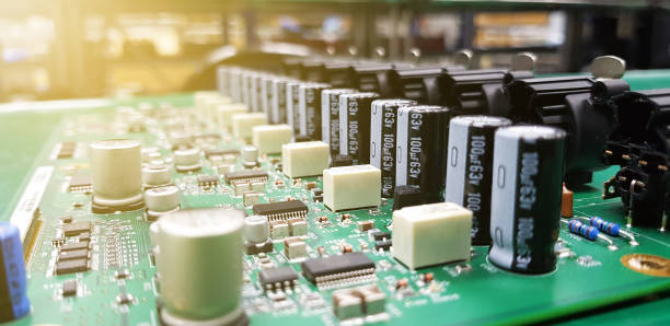
Before being deployed in real-world applications, high stability Image Processing PCB products require comprehensive testing and verification.
Testing procedures simulate actual operating conditions to identify potential reliability issues.
Key testing processes include:
Signal Transmission Testing
Signal integrity testing evaluates PCB performance under different image data rates, including:
- 2K transmission
- 4K transmission
- 8K transmission
Engineers analyze:
- Signal attenuation
- Transmission delay
- Data distortion
This ensures that image signals maintain accuracy throughout operation.
Environmental Reliability Testing
Environmental testing evaluates PCB performance under extreme conditions, including:
- High temperature
- Low temperature
- High humidity
- Mechanical vibration
For example, PCBs may be tested at low temperatures to verify signal stability and exposed to high humidity environments to confirm insulation performance.
Long-Term Reliability Testing
Long-term operation testing evaluates whether the PCB can maintain stable performance over extended periods.
These tests help identify:
- Material aging
- Electrical degradation
- Structural failures
Through comprehensive verification, manufacturers can ensure that PCBs meet demanding requirements for industrial imaging, medical equipment, and security applications.
Conclusion: High Stability Image Processing PCB Supports Next-Generation Imaging Systems
A high-performance Image Processing PCB is the foundation of reliable imaging systems. Its design directly determines signal integrity, image quality, and long-term operational stability.
From selecting suitable materials and applying effective protection layers to optimizing signal routing, improving thermal performance, and conducting strict reliability testing, every manufacturing step contributes to stable PCB performance.
With the continuous development of industrial automation, medical imaging, artificial intelligence vision, and security technologies, the demand for reliable PCB solutions continues to grow.
By partnering with an experienced manufacturer, companies can achieve better performance, improved reliability, and stronger competitiveness in advanced imaging applications.
Explore our High Reliability PCB solutions to develop stable and durable circuit boards for demanding industrial applications.
For complete PCB production support, including advanced design, manufacturing, and testing services, contact GoPCB for professional assistance.